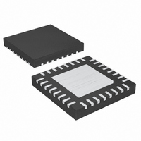
MAX5099ATJ+ Maxim Integrated Products, MAX5099ATJ+ Datasheet - Page 14

MAX5099ATJ+
Manufacturer Part Number
MAX5099ATJ+
Description
IC CONV BUCK SYNC DL 32TQFN-EP
Manufacturer
Maxim Integrated Products
Type
Step-Down (Buck)r
Datasheet
1.MAX5099ATJ.pdf
(27 pages)
Specifications of MAX5099ATJ+
Internal Switch(s)
Both
Synchronous Rectifier
Yes
Number Of Outputs
2
Voltage - Output
0.8 ~ 17.1 V
Current - Output
1A, 2A
Frequency - Switching
200kHz ~ 2.2MHz
Voltage - Input
4.5 ~ 19 V
Operating Temperature
-40°C ~ 125°C
Mounting Type
Surface Mount
Package / Case
32-TQFN Exposed Pad
Power - Output
2.76W
Output Voltage
5.2 V
Output Current
2 A
Input Voltage
5.2 V to 19 V
Supply Current
4.2 mA
Switching Frequency
1.9 MHz
Mounting Style
SMD/SMT
Maximum Operating Temperature
+ 125 C
Minimum Operating Temperature
- 40 C
Lead Free Status / RoHS Status
Lead free / RoHS Compliant
Dual, 2.2MHz, Automotive Synchronous Buck
Converter with 80V Load-Dump Protection
14
The MAX5099 dual DC-DC converters use a pulse-width-
modulation (PWM) voltage-mode control scheme. On
each converter the device includes one integrated n-
channel MOSFET switch and requires an external low-for-
ward-drop Schottky diode for output rectification. The
controller generates the clock signal by dividing down
the internal oscillator (f
ven by an external clock; therefore, each controller’s
switching frequency equals half the oscillator frequency
(f
f
produces an integrated error voltage at COMP_, provid-
ing high DC accuracy. The voltage at COMP_ sets
the duty cycle using a PWM comparator and a ramp
generator. At each rising edge of the clock, converter
1’s MOSFET switch turns on and remains on until either
the appropriate or maximum duty cycle is reached, or the
maximum current limit for the switch is reached.
Converter 2 operates 180° out-of-phase, so its MOSFET
switch turns on at each falling edge of the clock.
In the case of buck operation (see the Typical Application
Circuit ), the internal MOSFET is used in high-side config-
uration. During each MOSFET’s on-time, the associated
inductor current ramps up. During the second half of the
switching cycle, the high-side MOSFET turns off and for-
ward biases the Schottky rectifier. During this time, the
SOURCE_ voltage is clamped to a diode drop (V
ground. A low-forward-voltage-drop (0.4V) Schottky
diode must be used to ensure the SOURCE_ voltage
does not go below -0.6V absolute max. The inductor
releases the stored energy as its current ramps down,
and provides current to the output. The bootstrap capaci-
tor is also recharged when the SOURCE_ voltage goes
low during the high-side MOSFET off-time. The maximum
duty-cycle limits ensure proper bootstrap charging at
startup or low input voltages. The circuit goes in discon-
tinuous conduction mode operation at light load, when
the inductor current completely discharges before the
next cycle commences. Under overload conditions, when
the inductor current exceeds the peak current limit of the
respective switch, the high-side MOSFET turns off quickly
and waits until the next clock cycle.
The MAX5099 is intended mostly for synchronous buck
operation with an external synchronous-rectifier MOSFET.
During the internal high-side MOSFET on-time, the induc-
tor current ramps up. When the high-side MOSFET turns
off, the inductor reverses polarity and forward biases
the Schottky rectifier in parallel with the low-side external
SYNC
SW
______________________________________________________________________________________
= f
/2). An internal transconductance error amplifier
OSC
/2) or half of the SYNC input frequency (f
OSC
Detailed Description
Synchronous-Rectifier Output
) or the SYNC input when dri-
PWM Controller
D
) below
SW
=
synchronous MOSFET. The SOURCE_ voltage is
clamped to 0.5V below ground until the adaptive break-
before-make time (t
synchronous-rectifier MOSFET turns on, thus bypassing
the Schottky rectifier and reducing the conduction loss
during the inductor freewheeling time. The synchronous-
rectifier MOSFET keeps the circuit in continuous conduc-
tion mode operation even at light load because the
inductor current is allowed to go negative.
The MAX5099, with the synchronous-rectifier driver out-
put (DL_), has an adaptive break-before-make circuit
to avoid cross-conduction between the internal power
MOSFET and the external synchronous-rectifier MOSFET.
When the synchronous-rectifier MOSFET is turning off,
the internal high-side power MOSFET is kept off until V
falls below 0.97V. Similarly, DL_ does not go high until the
internal power MOSFET gate voltage falls below 1.24V.
Most automotive applications are powered by a multi-
cell, 12V lead-acid battery with a voltage from 9V to
16V (depending on load current, charging status, tem-
perature, battery age, etc.). The battery voltage is dis-
tributed throughout the automobile and is locally
regulated down to voltages required by the different
system modules. Load dump occurs when the alterna-
tor is charging the battery and the battery becomes
disconnected. Power in the alternator inductance flows
into the distributed power system and elevates the volt-
age seen at each module. The voltage spikes have rise
times typically greater than 5ms and decays within sev-
eral hundred milliseconds but can extend out to 1s or
more depending on the characteristics of the charging
system. These transients are capable of destroying
sensitive electronic equipment on the first fault event.
During load dump, the MAX5099 provides the ability to
clamp the input-voltage rail of the internal DC-DC con-
verters to a safe level, while preventing power disconti-
nuity at the DC-DC converters’ outputs.
The load-dump protection circuit utilizes an internal
charge pump to drive the gate of an external n-channel
MOSFET. This series-protection MOSFET absorbs the
load-dump overvoltage transient and operates in satu-
ration over the normal battery range to minimize power
dissipation. During load dump, the gate voltage of the
protection MOSFET is regulated to prevent the source
terminal from exceeding 19V.
The DC-DC converters are powered from the source
terminal of the load-dump protection MOSFET, so that
their input voltage is limited during load dump and can
operate normally.
BBM
) of 25ns is over. After t
Load-Dump Protection
BBM
, the
DL


