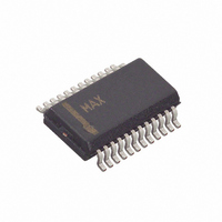
MAX1858EEG+ Maxim Integrated Products, MAX1858EEG+ Datasheet - Page 19

MAX1858EEG+
Manufacturer Part Number
MAX1858EEG+
Description
IC CNTRLR BUCK DUAL 24-QSOP
Manufacturer
Maxim Integrated Products
Type
Step-Down (Buck)r
Datasheet
1.MAX1858EEG.pdf
(21 pages)
Specifications of MAX1858EEG+
Internal Switch(s)
No
Synchronous Rectifier
No
Number Of Outputs
2
Voltage - Output
0 ~ 18 V
Current - Output
10A
Frequency - Switching
100kHz ~ 600kHz
Voltage - Input
4.75 ~ 23 V
Operating Temperature
-40°C ~ 85°C
Mounting Type
Surface Mount
Package / Case
24-QSOP
Power - Output
762mW
Lead Free Status / RoHS Status
Lead free / RoHS Compliant
• When trade-offs in trace lengths must be made,
• Ensure that the feedback connection to C
• Route high-speed switching nodes (BST_, LX_, DH_,
• Make all pin-strap control input connections (ILIM_,
1) Place the power components first, with ground termi-
by routing power to the MOSFETs from outside
using the top copper layer, while connecting PGND
and LX_ underneath the 8-pin SO package.
allow the inductor-charging path to be made longer
than the discharge path. Since the average input
current is lower than the average output current in
step-down converters, this minimizes the power dis-
sipation and voltage drops caused by board resis-
tance. For example, allow some extra distance
between the input capacitors and the high-side
MOSFET rather than to allow distance between the
inductor and the low-side MOSFET or between the
inductor and the output filter capacitor.
short and direct.
and DL_) away from the sensitive analog areas
(REF, COMP_, ILIM_, and FB_). Use PGND1 and
PGND2 as EMI shields to keep radiated noise away
from the IC, feedback dividers, and analog bypass
capacitors.
SYNC, and EN) to analog ground (GND) rather than
power ground (PGND).
nals adjacent (N
Controller with Power Sequencing and POR
______________________________________________________________________________________
Dual 180° Out-of-Phase PWM Step-Down
L
_ source, C
IN
Layout Procedure
_, and C
OUT
_). Make
OUT_
is
2) Mount the controller IC adjacent to the synchronous
3) Group the gate-drive components (BST_ diodes and
4) Make the DC-DC controller ground connections as
5) On the board’s top side (power planes), make a star
TRANSISTOR COUNT: 6688
PROCESS: BiCMOS
all these connections on the top layer with wide, cop-
per-filled areas (2oz copper recommended).
rectifier MOSFETs (N
side in order to keep LX_, PGND_, and DL_ traces
short and wide. The DL_ gate trace must be short
and wide, measuring 50mils to 100mils wide if the
low-side MOSFET is 1in from the controller IC.
capacitors, and V
the controller IC.
follows: create a small analog ground plane near the
IC. Connect this plane to GND and use this plane for
the ground connection for the reference (REF), V+
bypass capacitor, compensation components, feed-
back dividers, OSC resistor, and ILIM_ resistors (if
any). Connect GND and PGND together under the
IC (this is the only connection between GND and
PGND).
ground to minimize crosstalk between the two sides.
L
bypass capacitor) together near
L
_), preferably on the back
Chip Information
19


