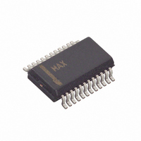
MAX1858EEG+ Maxim Integrated Products, MAX1858EEG+ Datasheet - Page 15

MAX1858EEG+
Manufacturer Part Number
MAX1858EEG+
Description
IC CNTRLR BUCK DUAL 24-QSOP
Manufacturer
Maxim Integrated Products
Type
Step-Down (Buck)r
Datasheet
1.MAX1858EEG.pdf
(21 pages)
Specifications of MAX1858EEG+
Internal Switch(s)
No
Synchronous Rectifier
No
Number Of Outputs
2
Voltage - Output
0 ~ 18 V
Current - Output
10A
Frequency - Switching
100kHz ~ 600kHz
Voltage - Input
4.75 ~ 23 V
Operating Temperature
-40°C ~ 85°C
Mounting Type
Surface Mount
Package / Case
24-QSOP
Power - Output
762mW
Lead Free Status / RoHS Status
Lead free / RoHS Compliant
removed from the output filter capacitors by a sudden
load step. The amount of output-voltage sag is also a
function of the maximum duty factor, which can be cal-
culated from the minimum off-time and switching fre-
quency:
where t
Electrical Characteristics), and f
the Setting the Switching Frequency section).
Each voltage-mode controller section employs a
transconductance error amplifier whose output is the
compensation point of the control loop. The control
loop is shown in Figure 7. For frequencies much lower
than Nyquist, the PWM block can be simplified to a
voltage amplifier. Connect R
COMP to GND to compensate the loop (see Figure 7).
The inductor, output capacitor, compensation resistor,
and compensation capacitors determine the loop sta-
bility. Since the inductor and output capacitor are cho-
sen based on performance, size, and cost, select the
compensation resistor and capacitors to optimize con-
trol-loop stability.
To determine the loop gain (A
FB to COMP (A
(A
gain is:
where:
assuming an ideal integrator, and assuming that
C
for frequencies lower than Nyquist.
COMP_B
LX/COMP
V
SAG
OFF(MIN)
A
=
A
L
is much less than C
Controller with Power Sequencing and POR
), and from LX to FB (A
L I
COMP FB
A
=
(
2
LOAD
LX COMP
A
C
COMP FB
OUT OUT
/
/
______________________________________________________________________________________
1
is the minimum off-time (see the
Dual 180° Out-of-Phase PWM Step-Down
-
V
COMP/FB
I
LOAD
=
/
×
V
=
COMP
1
V
1
×
V
FB
+
+
COMP
2
A
V
sR
V
sR
)
LX COMP
LX
2
IN
COMP_
V f
COMP COMP A
COMP_A
L
), from COMP to LX
COMP COMP B
IN SW
/
-
≅
), consider the gain from
V f
V
SW
V
g
=
IN SW
OUT
SC
OUT
M COMP
FB/LX
V
_
C
C
is set by R
RAMP
and C
COMP
V
Compensation
×
IN
.
+
-
A
). The total loop
t
FB LX
OFF MIN
t
OFF MIN
COMP_A
/
_
_
(
(
OSC
)
)
from
(see
Therefore:
For an ideal integrator, this loop gain approaches infini-
ty at DC. In reality the g
impedance which imposes a finite, but large, loop gain.
It is this large loop gain that provides DC load accura-
cy. The dominant pole occurs due to the integrator, and
for this analysis, it can be approximated to occur at DC.
R
The inductor and capacitor form a double pole at:
At some higher frequency the output capacitor’s
impedance becomes insignificant compared to its ESR,
and the LC system becomes more like an LR system,
turning a double pole into a single pole. This zero
occurs at:
A final pole is added using C
gain and attenuate noise after crossover. This pole
(f
Figure 8 shows a Bode plot of the poles and zeros in
their relative locations.
Near crossover the following approximations can be
made to simplify the loop-gain equation:
f
A
Z COMP A
COMP_B
COMP
A
L
_
FB LX
×
≅
V
/
V
f
SC
COMP B
g
OUT
SET
creates a zero at:
M COMP
) occurs at:
COMP A
≅
_
=
_
V
V
V
V
×
_
OUT
FB
LX
=
SET
1
f
ESR
2π
+
S LC
_
f
=
LC
=
2
SR
×
2π
V
V
V
1
=
OUT
R
=
OUT
×
SET
ESR OUT
+
×
COMP
2π
2π
OUT
1
1
SR
R
+
+
S LC
COMP COMP B
C
×
×
SR
S LC
SR
2
ESR OUT
M
R
2
1
+
_
ESR OUT
LC
1
COMP COMP A
COMP COMP B
1
amplifier has a finite output
C
1
1
C
OUT
C
COMP A
OUT
OUT
1
C
+
COMP_B
sR
+
C
C
+
1
_
ESR OUT
SR
_
ESR OUT
C
_
_
to reduce the
C
×
V
RAMP
+
V
IN
1
15


