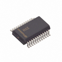
MAX1858EEG+ Maxim Integrated Products, MAX1858EEG+ Datasheet - Page 17

MAX1858EEG+
Manufacturer Part Number
MAX1858EEG+
Description
IC CNTRLR BUCK DUAL 24-QSOP
Manufacturer
Maxim Integrated Products
Type
Step-Down (Buck)r
Datasheet
1.MAX1858EEG.pdf
(21 pages)
Specifications of MAX1858EEG+
Internal Switch(s)
No
Synchronous Rectifier
No
Number Of Outputs
2
Voltage - Output
0 ~ 18 V
Current - Output
10A
Frequency - Switching
100kHz ~ 600kHz
Voltage - Input
4.75 ~ 23 V
Operating Temperature
-40°C ~ 85°C
Mounting Type
Surface Mount
Package / Case
24-QSOP
Power - Output
762mW
Lead Free Status / RoHS Status
Lead free / RoHS Compliant
Figure 8. Voltage-Mode Loop Analysis
All four N-channel MOSFETs must be a logic-level type
with guaranteed on-resistance specifications at V
4.5V. For maximum efficiency, choose a high-side
MOSFET (N
switching losses at the optimum input voltage. Check to
ensure that the conduction losses at minimum input
voltage do not exceed MOSFET package thermal limits,
or violate the overall thermal budget. Also, check to
ensure that the conduction losses plus switching losses
at the maximum input voltage do not exceed package
ratings or violate the overall thermal budget.
Ensure that the MAX1858 DL _ gate driver can drive
N
turning on does not pull up the N
drain-to-gate capacitance. This is the most frequent
cause of cross-conduction problems.
Gate-charge losses are dissipated by the driver and do
not heat the MOSFET. All MOSFETs must be selected
so that their total gate charge is low enough that V
power all four drivers without overheating the IC:
MOSFET package power dissipation often becomes a
dominant design factor. I
est heat contributor for both high-side and low-side
MOSFETs. I
N
below. Switching losses affect only the high-side
MOSFET, since the low-side MOSFET is a zero-voltage
switched device when used in the buck topology.
L
L
_. In particular, check that the dv/dt caused by N
_ according to duty factor as shown in the equations
-10
-20
-30
-40
50
40
30
20
10
Controller with Power Sequencing and POR
0
0.001
H
2
P
R losses are distributed between N
_) that has conduction losses equal to the
VL
f
Z-COMP_A
=
BODE PLOT FOR VOLTAGE-
______________________________________________________________________________________
V
Dual 180° Out-of-Phase PWM Step-Down
IN
MODE CONTROLLERS
×
0.01
FREQUENCY (MHz)
Q
f
LC
2
G TOTAL
R power losses are the great-
_
f
f
ESR
COMP_B
f
CO
0.1
L
_ gate through N
×
f
SW
f
SWITCH
1
H
_ and
L
GS
L
can
_’s
H
≥
_
Calculate MOSFET temperature rise according to pack-
age thermal-resistance specifications to ensure that
both MOSFETs are within their maximum junction tem-
perature at high ambient temperature. The worst-case
dissipation for the high-side MOSFET (P
both extremes of input voltage, and the worst-case dis-
sipation for the low-side MOSFET (P
mum input voltage.
I
determined by:
where R
resistance (5Ω max), and R
tance between DH and BST (Figure 3).
where P
in the high-side MOSFET, and P
power loss.
To reduce EMI caused by switching noise, add a 0.1µF
ceramic capacitor from the high-side switch drain to
the low-side switch source or add resistors in series
with DL_ and DH_ to increase the MOSFETs’ turn-on
and turn-off times.
When working with low input voltages, the output-voltage
adjustable range for continuous-conduction operation is
restricted by the minimum off-time (t
dropout performance, use the lowest (100kHz) switching-
frequency setting. Manufacturing tolerances and internal
propagation delays introduce an error to the switching
frequency and minimum off-time specifications. This error
is more significant at higher frequencies. Also, keep in
mind that transient response performance of buck regula-
tors operated close to dropout is poor, and bulk output
P
GATE
NH SWITCHING
P
P
P
NH CONDUCTION
NH TOTAL
NL
(
(
(
is the average DH driver output current capability
=
I
DS(ON)DH
NH(CONDUCTION)
LOAD
I
GATE
)
2
=
R
P
)
Applications Information
DS ON NL
NH SWITCHING
=
=
2
is the high-side MOSFET driver’s on-
(
V I
(
)
(
IN LOAD OSC
R
=
DS ON DH
)
I
LOAD
(
2
is the conduction power loss
1-
f
)
Dropout Performance
2
V
R
GATE
L
DS ON NH
V
)
V
OUT
+
+
IN
NL
(
R
P
Q
NH CONDUCTION
GATE
is any series resis-
GS
is the total low-side
NL
)
OFF(MIN)
I
(
GATE
) occurs at maxi-
+
)
Q
V
NH
GD
OUT
V
IN
) occurs at
). For best
)
17


