ISL8501IRZ Intersil, ISL8501IRZ Datasheet - Page 7
ISL8501IRZ
Manufacturer Part Number
ISL8501IRZ
Description
IC CTLR TRPL PWM/DUAL LDO 24-QFN
Manufacturer
Intersil
Type
Step-Down (Buck)r
Datasheet
1.ISL8501IRZ.pdf
(19 pages)
Specifications of ISL8501IRZ
Internal Switch(s)
Yes
Synchronous Rectifier
No
Number Of Outputs
3
Voltage - Output
0.6 ~ 20 V
Current - Output
1A
Frequency - Switching
500kHz
Voltage - Input
5V, 6 ~ 25 V
Operating Temperature
-40°C ~ 85°C
Mounting Type
Surface Mount
Package / Case
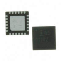
24-VQFN
Rohs Compliant
YES
Lead Free Status / RoHS Status
Lead free / RoHS Compliant
Power - Output
-
Available stocks
Company
Part Number
Manufacturer
Quantity
Price
Company:

Part Number:
ISL8501IRZ
Manufacturer:
Intersil
Quantity:
275


Pin Descriptions
VIN
The input supply for the PWM regulator power stage and the
source for the internal linear regulator that provides bias for
the IC. Place a ceramic capacitor from VIN to GND, close to
the IC for decoupling (typical 1μF).
PVCC
Connect this pin to VCC.
GND
Ground connect for the IC and thermal relief for the package.
The exposed pad must be connected to GND and soldered
to the PCB. All voltage levels are measured with respect to
this pin.
VCC
Internal 5V linear regulator output provides bias to all the
internal control logic. The ISL8501 may be powered directly
from a 5V (±10%) supply at this pin. When used as a 5V
supply input, this pin must be externally connected to VIN.
The VCC pin must always be decoupled to GND with a
ceramic bypass capacitor (minimum 1μF) located close to
the pin.
FB and COMP
The standard buck regulator employs a single voltage
control loop. FB is the negative input to the voltage loop error
amplifier. COMP is the output of the error amplifier. The
output voltage is set by an external resistor divider
connected to FB. With a properly selected divider, the output
voltage can be set to any voltage between the power rail
(reduced by converter losses) and the 0.6V reference.
Connecting an AC network across COMP and FB provide
loop compensation to the amplifier.
In addition, the PWM regulator power good and under-
voltage protection circuitry use FB to monitor the regulator
output voltage.
PHASE
Switch node connections to internal power MOSFET source,
external output inductor, and external diode cathode.
BOOT
Floating bootstrap supply pin for the power MOSFET gate
driver. The bootstrap capacitor provides the necessary
charge to turn and hold on the internal N-Channel MOSFET.
Connect an external capacitor from this pin to PHASE.
6V to 25V
5V ±10%
INPUT
TABLE 1. INPUT SUPPLY CONFIGURATION
Connect the input supply to the VIN pin only. The
VCC pin will provide a 5V output from the internal
linear regulator.
Connect the input supply to the VIN and VCC pins.
PIN CONFIGURATION
7
ISL8501
EN
PWM controller enable input. The PWM converter and
LDO's outputs are held off when the pin is pulled to ground.
When the voltage on this pin rises above 1.7V, the chip is
enabled.
SS
Program pin for soft-start duration. A regulated 30μA pull-up
current source charges a capacitor connected from the pin to
GND. The output voltage of the converter follows the
ramping voltage on the SS pin.
VIN_LDO1, VIN_LDO2
Input voltage pin for each LDO.
VOUT1, VOUT2
LDO output pins. Bypass with a minimum of 2.2μF, low ESR
capacitor to GND for stable operation.
FB_LDO1, FB_LDO2
Used to set the output of LDO with the proper selection of
resistor divider. The resistors should be selected to provide a
minimum current of 200nA load for the LDO.
CC1, CC2
Compensation capacitor connection for each LDO. Connect
a 0.033μF capacitor from each pin to ground.
EN_LDO1, EN_LDO2
These pins are threshold-sensitive enable inputs for the
individual LDOs. Held low, this pin disables the respective
LDO.
PG_PWM
PWM converter power good output. Open drain logic output
that is pulled to ground when the output voltage is outside
regulation limits. Connect a 100kΩ resistor from this pin to
VCC. Pin is low when the buck regulator output voltage is
not within 10% of the respective nominal voltage, or during
the soft-start interval. Pin is high impedance when the output
is within regulation.
PG_LDO
Combined LDO power good output. Connect a 100kΩ
resistor from this pin to VCC.
July 12, 2007
FN6500.1
Related parts for ISL8501IRZ
Image
Part Number
Description
Manufacturer
Datasheet
Request
R

Part Number:
Description:
Triple Output Controller With 1a Standard Buck Pwm And Dual Ldos
Manufacturer:
Intersil Corporation
Datasheet:
Part Number:
Description:
Intersil Corporation [CMOS Serial Controller Interface]
Manufacturer:
Intersil Corporation
Datasheet:
Part Number:
Description:
Manufacturer:
Intersil Corporation
Datasheet:
Part Number:
Description:
357-036-542-201 CARDEDGE 36POS DL .156 BLK LOPRO
Manufacturer:
Intersil Corporation
Datasheet:
Part Number:
Description:
1024-Word x 4-Bit LSI Static RAM
Manufacturer:
Intersil Corporation
Datasheet:
Part Number:
Description:
General Purpose NPN Transistor Arrays FN341.4
Manufacturer:
Intersil Corporation
Datasheet:
Part Number:
Description:
CMOS 16-Bit Microprocessor
Manufacturer:
Intersil Corporation
Datasheet:
Part Number:
Description:
Manufacturer:
Intersil Corporation
Datasheet:
Part Number:
Description:
Manufacturer:
Intersil Corporation
Datasheet:
Part Number:
Description:
Manufacturer:
Intersil Corporation
Datasheet:
Part Number:
Description:
Manufacturer:
Intersil Corporation
Datasheet:
Part Number:
Description:
CMOS 6-Bit Latch and Decoder Memory Interfaces
Manufacturer:
Intersil Corporation
Datasheet:
Part Number:
Description:
CA3046General Purpose NPN Transistor Arrays
Manufacturer:
Intersil Corporation
Datasheet:
Part Number:
Description:
Manufacturer:
Intersil Corporation
Datasheet:
Part Number:
Description:
TR909 DLC/FLC SLIC with Low Power Standby
Manufacturer:
Intersil Corporation
Datasheet: