ISL8501IRZ Intersil, ISL8501IRZ Datasheet
ISL8501IRZ
Specifications of ISL8501IRZ
Available stocks


Related parts for ISL8501IRZ

ISL8501IRZ Summary of contents
Page 1
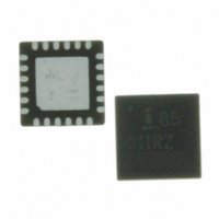
... TEMP. PACKAGE (Note) MARKING RANGE (°C) ISL8501IRZ* 85 01IRZ - 4x4 QFN L24.4x4D *Add “-T” suffix for tape and reel NOTE: Intersil Pb-free plus anneal products employ special Pb-free material sets; molding compounds/die attach materials and 100% matte tin plate termination finish, which are RoHS compliant and compatible with both SnPb and Pb-free soldering operations ...
Page 2
Typical Application Schematics R5 FB_LDO1 5.11k R6 LDO1 5.11k 1. μ F VIN_LDO1 VOUT1 C7 10 μ F VIN_LDO2 LDO2 VOUT2 1. μ 5.11k FB_LDO2 R8 2.55k 2 ISL8501 R2 2.21k C4 C5 0.1 ...
Page 3
Typical Application Schematics R5 FB_LDO1 5.11k R6 LDO1 5.11k 1. μ F VIN_LDO1 VOUT1 C7 10 μ F VIN_LDO2 LDO2 VOUT2 1. μ 5.11k FB_LDO2 R8 2.55k 3 ISL8501 (Continued) R2 2.21k C4 C5 ...
Page 4
Functional Block Diagram VCC SOFT-START CONTROL 30μ EN_LDO1 EN_LDO2 VIN LDO VCC PG_PWM PG_LDO GND 4 ISL8501 - VOLTAGE + MONITOR EA 0.6V RAMP REFERENCE GENERATOR FAULT MONITOR THERMAL MONITOR OSCILLATOR o +150 C OC MONITOR PVCC POWER-ON ...
Page 5
... Maximum Storage Temperature Range . . . . . . . . . .-65°C to +150°C Junction Temperature Range .-55°C to +150°C Storage Temperature Range . . . . . . . . . . . . . . . . . .-65°C to +150°C Operating Temperature Range . . . . . . . . . . . . . . . . .-40°C to +85°C Pb-free reflow profile . . . . . . . . . . . . . . . . . . . . . . . . . .see link below http://www.intersil.com/pbfree/Pb-FreeReflow.asp SYMBOL TEST CONDITIONS VIN VIN connected to VCC (Note 6) ...
Page 6
Electrical Specifications Unless Otherwise Noted, All Parameter Limits are Guaranteed Over the Recommended Operating Conditions and the Typical Specifications are Measured at the Following Conditions 25V, Unless Otherwise Noted. Typical Values are ...
Page 7
Pin Descriptions VIN The input supply for the PWM regulator power stage and the source for the internal linear regulator that provides bias for the IC. Place a ceramic capacitor from VIN to GND, close to the IC for decoupling ...
Page 8
Typical Performance Curves 100 1.8V 60 OUT 2.5V OUT 1.5V 50 OUT 40 1.2V OUT 0.00 0.25 0.50 0.75 OUTPUT LOAD (A) FIGURE 3. EFFICIENCY vs LOAD 3.3V ...
Page 9
Typical Performance Curves 2.503 2.503 2.502 2.502 2.501 12V IN 2.501 2.500 0.00 0.25 0.50 0.75 OUTPUT LOAD (A) FIGURE 9. V REGULATION vs LOAD, 500kHz 2.5V OUT 5.015 5.014 5.013 7V IN 5.012 5.011 5.010 5.009 5.008 12V IN ...
Page 10
Typical Performance Curves 5.1 5.0 4.9 4.8 4.7 4.6 4.5 4 100 I V (mA) CC FIGURE 15. V LOAD REGULATION CC 1.30 1. 1.26 1.24 12V IN 1.22 1.20 1.18 1.16 1.14 1.12 1.10 0 ...
Page 11
Typical Performance Curves IL 1A/DIV LDO1 RIPPLE 20mV/DIV FIGURE 21. LOAD TRANSIENT, 200µs/DIV EN 5V/DIV IL 1A/DIV PG_PWM 2V/DIV SS 2V/DIV FIGURE 23. SOFT-START AT FULL LOAD, 500µs/DIV EN 5V/DIV IL 1A/DIV PG_PWM 5V/DIV FIGURE 25. SHUT DOWN CIRCUIT AT ...
Page 12
... Accordingly, the reader is cautioned to verify that data sheets are current before placing orders. Information furnished by Intersil is believed to be accurate and reliable. However, no responsibility is assumed by Intersil or its subsidiaries for its use; nor for any infringements of patents or other rights of third parties which may result from its use ...
Page 13
Detailed Description The ISL8501 combines a standard buck PWM controller with an integrated switching MOSFET and two low dropout (LDO) linear regulators with internal pass devices. The buck controller drives an internal N-Channel MOSFET and requires an external diode to ...
Page 14
The voltage on SS begins ramping linearly from ground until the voltage across the soft-start capacitor reaches 3.0V. This linear ramp is applied to the non-inverting input of the internal error amplifier and overrides the ...
Page 15
LDO Current Limit The ISL8501 monitors and controls the pass transistor’s gate voltage to limit output current. The current limit for both LDO1 and LDO2 is 700mA typical. The output can be shorted to ground without damaging the part due ...
Page 16
For stable operation, a ceramic capacitor, with a minimum value of 10µF, is recommended for both LDO outputs. There is no upper limit to the output capacitor value. Larger capacitor can reduce noise and improve load transient ...
Page 17
The important parameters for the bulk input capacitance are the voltage rating and the RMS current rating. For reliable operation, select bulk capacitors with voltage and current ratings above the maximum input voltage and largest RMS current required by the ...
Page 18
The compensation gain uses external impedance networks Z and Z to provide a stable, high bandwidth (BW) overall FB IN loop. A stable control loop has a gain crossing with -20dB/decade slope and a phase margin greater than 45°. Include ...
Page 19
Package Outline Drawing L24.4x4D 24 LEAD QUAD FLAT NO-LEAD PLASTIC PACKAGE Rev 2, 10/06 4.00 PIN 1 INDEX AREA (4X) 0.15 TOP VIEW ( TYP ) ( TYPICAL RECOMMENDED LAND PATTERN 19 ISL8501 ...