ISL8501IRZ Intersil, ISL8501IRZ Datasheet - Page 17
ISL8501IRZ
Manufacturer Part Number
ISL8501IRZ
Description
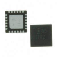
IC CTLR TRPL PWM/DUAL LDO 24-QFN
Manufacturer
Intersil
Type
Step-Down (Buck)r
Datasheet
1.ISL8501IRZ.pdf
(19 pages)
Specifications of ISL8501IRZ
Internal Switch(s)
Yes
Synchronous Rectifier
No
Number Of Outputs
3
Voltage - Output
0.6 ~ 20 V
Current - Output
1A
Frequency - Switching
500kHz
Voltage - Input
5V, 6 ~ 25 V
Operating Temperature
-40°C ~ 85°C
Mounting Type
Surface Mount
Package / Case
24-VQFN
Rohs Compliant
YES
Lead Free Status / RoHS Status
Lead free / RoHS Compliant
Power - Output
-
Available stocks
Company
Part Number
Manufacturer
Quantity
Price
Company:

Part Number:
ISL8501IRZ
Manufacturer:
Intersil
Quantity:
275


The important parameters for the bulk input capacitance are
the voltage rating and the RMS current rating. For reliable
operation, select bulk capacitors with voltage and current
ratings above the maximum input voltage and largest RMS
current required by the circuit. Their voltage rating should be
at least 1.25 times greater than the maximum input voltage,
while a voltage rating of 1.5 times is a conservative
guideline. For most cases, the RMS current rating
requirement for the input capacitor of a buck regulator is
approximately 1/2 the DC load current.
The maximum RMS current required by the regulator may be
closely approximated through the Equation 6:
For a through hole design, several electrolytic capacitors
may be needed. For surface mount designs, solid tantalum
capacitors can be used, but caution must be exercised wih
regard to the capacitor surge current rating. These
capacitors must be capable of handling the surge-current at
power-up. Some capacitor series available from reputable
manufacturers are surge current tested.
Feedback Compensation
Figure 2 highlights the voltage-mode control loop for a
synchronous-rectified buck converter. The output voltage
(V
amplifier output (V
triangular wave to provide a pulse-width modulated (PWM)
wave with an amplitude of V
PWM wave is smoothed by the output filter (L
The modulator transfer function is the small-signal transfer
function of V
Gain and the output filter (L
break frequency at f
the modulator is simply the input voltage (V
peak-to-peak oscillator voltage ΔV
Modulator Break Frequency Equations
The compensation network consists of the error amplifier
(internal to the ISL8501) and the impedance networks Z
and Z
a closed loop transfer function with the highest 0dB crossing
frequency (f
is the difference between the closed loop phase at f
180°. The following equations relate the compensation
network’s poles, zeros and gain to the components (R
R
locating the poles and zeros of the compensation network:
f LC
I
1. Pick Gain (R
RMS MAX
4
OUT
, C
=
1
FB
------------------------------------------ -
2π x
) is regulated to the Reference voltage level. The error
, C
. The goal of the compensation network is to provide
=
2
, and C
0dB
L O x C O
OUT
V
------------- -
1
V
OUT
IN
) and adequate phase margin. Phase margin
2
/V
/R
×
E/A
3
E/A
) in Figure 2. Use these guidelines for
⎛
⎝
LC
1
I
) for desired converter bandwidth.
OUT MAX
) is compared with the oscillator (OSC)
. This function is dominated by a DC
and a zero at f
O
IN
2
17
f ESR
and C
+
at the PHASE node. The
----- -
12
1
OSC
×
=
O
⎛
⎝
------------------------------------------- -
2π x ESR x C O
V
---------------------------- -
), with a double pole
ESR
IN
.
L
–
×
V
. The DC Gain of
IN
f
1
OUT
s
) divided by the
O
×
and C
V
------------- -
V
OUT
IN
0dB
(EQ. 7)
1
(EQ. 6)
O
⎞
⎠
2
, R
).
and
⎞
⎠
IN
2
,
ISL8501
Compensation Break Frequency Equations
Figure 3 shows an asymptotic plot of the DC/DC converter’s
gain vs frequency. The actual Modulator Gain has a high
gain peak due to the high Q factor of the output filter and is
not shown in Figure 3. Using the guidelines from “Modulator
Break Frequency Equations” on page 17 should give a
Compensation Gain similar to the curve plotted. The open
loop error amplifier gain bounds the compensation gain.
Check the compensation gain at f
the error amplifier. The Closed Loop Gain is constructed on
the graph of Figure 33 by adding the Modulator Gain (in dB)
to the Compensation Gain (in dB). This is equivalent to
multiplying the modulator transfer function to the
compensation transfer function and plotting the gain.
f
f
2. Place1 st Zero Below Filter’s Double Pole (~75% f
3. Place 2nd Zero at Filter’s Double Pole.
4. Place 1st Pole at the ESR Zero.
5. Place 2nd Pole at Half the Switching Frequency.
6. Check Gain against Error Amplifier’s Open-Loop Gain.
7. Estimate Phase Margin - Repeat if Necessary.
Z1
Z2
ΔV
FIGURE 32. VOLTAGE-MODE BUCK CONVERTER
OSC
=
=
----------------------------------- -
2π x R
------------------------------------------------------ -
2π x R
OSC
(
1
4
1
COMPARATOR
COMPENSATION DESIGN AND OUTPUT
VOLTAGE SELECTION
x C
1
+
ERROR
AMP
DETAILED COMPENSATION COMPONENTS
V
ISL8501
R
E/A
2
PWM
3
) x C
Z
+
-
-
+
FB
COMP
C
REFERENCE
1
2
REFERENCE
C
-
+
3
f
f
DRIVER
DRIVER
R
P1
P2
Z
4
IN
=
=
P2
-------------------------------------------------------- -
2π x R
----------------------------------- -
2π x R
FB
with the capabilities of
Z
FB
PHASE
R
(PARASITIC)
1
V
2
C
4
3
IN
1
x
x C
L
Z
R
1
IN
O
⎛
⎜
⎝
1
C
--------------------- -
C
1
R
ESR
3
3
C
3
+
x C
O
V
DDQ
C
July 12, 2007
LC
2
2
(EQ. 8)
FN6500.1
⎞
⎟
⎠
).
V
DDQ
Related parts for ISL8501IRZ
Image
Part Number
Description
Manufacturer
Datasheet
Request
R

Part Number:
Description:
Triple Output Controller With 1a Standard Buck Pwm And Dual Ldos
Manufacturer:
Intersil Corporation
Datasheet:
Part Number:
Description:
Intersil Corporation [CMOS Serial Controller Interface]
Manufacturer:
Intersil Corporation
Datasheet:
Part Number:
Description:
Manufacturer:
Intersil Corporation
Datasheet:
Part Number:
Description:
357-036-542-201 CARDEDGE 36POS DL .156 BLK LOPRO
Manufacturer:
Intersil Corporation
Datasheet:
Part Number:
Description:
1024-Word x 4-Bit LSI Static RAM
Manufacturer:
Intersil Corporation
Datasheet:
Part Number:
Description:
General Purpose NPN Transistor Arrays FN341.4
Manufacturer:
Intersil Corporation
Datasheet:
Part Number:
Description:
CMOS 16-Bit Microprocessor
Manufacturer:
Intersil Corporation
Datasheet:
Part Number:
Description:
Manufacturer:
Intersil Corporation
Datasheet:
Part Number:
Description:
Manufacturer:
Intersil Corporation
Datasheet:
Part Number:
Description:
Manufacturer:
Intersil Corporation
Datasheet:
Part Number:
Description:
Manufacturer:
Intersil Corporation
Datasheet:
Part Number:
Description:
CMOS 6-Bit Latch and Decoder Memory Interfaces
Manufacturer:
Intersil Corporation
Datasheet:
Part Number:
Description:
CA3046General Purpose NPN Transistor Arrays
Manufacturer:
Intersil Corporation
Datasheet:
Part Number:
Description:
Manufacturer:
Intersil Corporation
Datasheet:
Part Number:
Description:
TR909 DLC/FLC SLIC with Low Power Standby
Manufacturer:
Intersil Corporation
Datasheet: