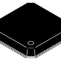
ADP3208DJCPZ-RL ON Semiconductor, ADP3208DJCPZ-RL Datasheet - Page 20

ADP3208DJCPZ-RL
Manufacturer Part Number
ADP3208DJCPZ-RL
Description
IC CTLR BUCK 7BIT 2PHASE 48LFCSP
Manufacturer
ON Semiconductor
Datasheet
1.ADP3208DJCPZ-RL.pdf
(37 pages)
Specifications of ADP3208DJCPZ-RL
Applications
Controller, Power Supplies for Next-Generation Intel Processors
Voltage - Input
3.3 ~ 22 V
Number Of Outputs
1
Voltage - Output
0.01 ~ 1.5 V
Operating Temperature
-10°C ~ 100°C
Mounting Type
Surface Mount
Package / Case
48-LFCSP
Output Voltage
10 mV
Output Current
40 A
Input Voltage
19 V
Supply Current
6 mA
Switching Frequency
300 KHz
Mounting Style
SMD/SMT
Maximum Operating Temperature
+ 100 C
Minimum Operating Temperature
- 10 C
Lead Free Status / RoHS Status
Lead free / RoHS Compliant
Available stocks
Company
Part Number
Manufacturer
Quantity
Price
Company:
Part Number:
ADP3208DJCPZ-RL
Manufacturer:
ON Semiconductor
Quantity:
10
Part Number:
ADP3208DJCPZ-RL
Manufacturer:
ON/安森美
Quantity:
20 000
operation, the voltage on the I
pin. The voltage across R
the CSA (from CSREF pin to CSCOMP pin). This voltage
is proportional to output current. The current through R
is proportional to the output inductor current. The current
through R
current. When the R
reference current, the ADP3208D goes into current limit.
The current limit circuit is shown in Figure 30.
a secondary current limit is activated. This is necessary
because the voltage swing on CSCOMP cannot extend
below ground. The secondary current limit circuit clamps
the internal COMP voltage and sets the internal
compensation ramp termination voltage at 1.5 V level. The
clamp actually limits voltage drop across the low side
MOSFETs through the current balance circuitry.
phases in case one or more phases stop functioning because
of a faulty component. This limit is based on the maximum
normal mode COMP voltage.
The latchoff can be reset by removing and reapplying VCC,
or by recycling the EN pin low and high for a short time.
VCC, or by recycling the EN pin low and high for a short
time.
CLA
20 μA
During startup when the output voltage is below 200 mV,
An inherent per phase current limit protects individual
After 9 ms in current limit, the ADP3208D will latchoff.
The latchoff can be reset by removing and reapplying
+
-
R
LIM
I
R
ILIM
LIM
R
Figure 30. Current Limit Circuit
LIM
Figure 31. Current Overload
CURRENT LIMIT
is compared with an internal reference
I
LIM
APPLIED
CSCOMP
LIM
CSA
R
CS
C
OUTPUT 0.5 V/DIV
CS
PWRGD 2.0 V/DIV
LIM
+
-
current goes above the internal
2 ms/DIV
VI CONV
+
-
LIM
is equal to the voltage across
CSSUM
R
CSREF
PH
pin is equal to the CSREF
LATCHED
OFF
L
DCR
http://onsemi.com
C
BULK
LIM
20
Changing VID OTF
changing VID code. As a consequence, the CPU VCC
voltage can change without the need to reset the controller
or the CPU. This concept is commonly referred to as VID
OTF transient. A VID OTF can occur with either light or
heavy load conditions. The processor alerts the controller
that a VID change is occurring by changing the VID inputs
in LSB incremental steps from the start code to the finish
code. The change can be either upwards or downwards steps.
change but ignores new code for a minimum of 400 ns. This
delay is required to prevent the device from reacting to
digital signal skew while the 7−bit VID input code is in
transition. Additionally, the VID change triggers a PWRGD
masking timer to prevent a PWRGD failure. Each VID
change resets and retriggers the internal PWRGD masking
timer.
ADP3208D forces PWM mode regardless of the state of the
system input signals. For example, this means that if the chip
is configured as a dual−phase controller but is running in
single−phase mode due to a light load condition, a current
overload event causes the chip to switch to dual−phase mode
to share the excessive load until the delayed current limit
latchoff cycle terminates.
runs in RPM mode. When a VID transition occurs, however,
the ADP3208D switches to dual−phase PWM mode.
Light Load RPM DCM Operation
the APD3208 operates in Continuous Conduction Mode
(CCM) over the entire load range. The upper and lower
MOSFETs run synchronously and in complementary phase.
See Figure 32 for the typical waveforms of the ADP3208D
running in CCM with a 7 A load current.
The ADP3208D is designed to track dynamically
When a VID input changes, the ADP3208D detects the
As listed in Table 3, during a VID transient, the
In user−set single−phase mode, the ADP3208D usually
In single−phase normal mode, DPRSLP is pulled low and
Figure 32. Single−Phase Waveforms in CCM
4
2
3
1
SWITCH NODE 5.0 V/DIV
LOW−SIDE GATE 5.0 V/DIV
INDUCTOR CURRENT 5 A/DIV
OUTPUT VOLTAGE 20 mV/DIV
400 ns/DIV


