LM96194CISQ/NOPB National Semiconductor, LM96194CISQ/NOPB Datasheet - Page 102
LM96194CISQ/NOPB
Manufacturer Part Number
LM96194CISQ/NOPB
Description
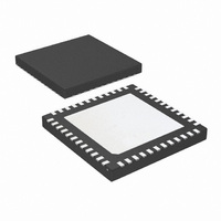
IC TRUTHERM HDWR MONITOR 48-LLP
Manufacturer
National Semiconductor
Series
PowerWise®, TruTherm®r
Datasheet
1.LM96194CISQNOPB.pdf
(106 pages)
Specifications of LM96194CISQ/NOPB
Function
Fan Control, Temp Monitor
Topology
ADC (Sigma Delta), Comparator, Fan Control, Multiplexer, Register Bank
Sensor Type
External & Internal
Sensing Temperature
-40°C ~ 85°C, External Sensor
Output Type
SMBus™
Output Alarm
No
Output Fan
Yes
Voltage - Supply
3 V ~ 3.6 V
Operating Temperature
-40°C ~ 85°C
Mounting Type
Surface Mount
Package / Case
48-LLP
Lead Free Status / RoHS Status
Lead free / RoHS Compliant
Other names
LM96194CISQTR


www.national.com
PROCHOT
GND
GND
GND
GND
GND
GPIO_0/TACH1
GPIO_1/TACH2
GPIO_2/TACH3
GPIO_3/TACH4
GPIO_4 /THERMTRIP
GPIO_5
GPIO_6
GPIO_7
VRD_HOT
GND
SCSI_TERM1
SMBDAT
SMBCLK
ALERT/XtestOut
RESET
AGND
REMOTE1–
REMOTE1+
REMOTE2–
REMOTE+
AD_IN1
AD_IN2
AD_IN3
Note 1: Absolute Maximum Ratings indicate limits beyond which damage to the device may occur. Operating Ratings indicate conditions for which the device is
functional, but do not guarantee specific performance limits. For guaranteed specifications and test conditions, see the Electrical Characteristics. The guaranteed
specifications apply only for the test conditions listed. Some performance characteristics may degrade when the device is not operated under the listed test
conditions.
Note 2: All voltages are measured with respect to GND, unless otherwise noted.
Note 3: When the input voltage (V
at that pin should be limited to 10 mA. The 100 mA maximum package input current rating limits the number of pins that can safely exceed the power supplies
with an input current of 10 mA to ten. Parasitic components and/or ESD protection circuitry are shown below for the LM96194’s pins. Care should be taken not
to forward bias the parasitic diode, D1, present on pins D+ and D− as shown in circuits C and D. Doing so by more than 50 mV may corrupt temperature
measurements. D1 and the ESD Clamp are connected between V+ (V
Symbol
IN
) at any pin exceeds the power supplies (V
Pin #
10
11
12
13
14
15
16
17
18
19
20
21
22
23
24
25
26
27
28
29
1
2
3
4
5
6
7
8
9
shorted to GND
B (Internally
Circuit
pin.)
DD
C
D
C
D
D
D
D
A
A
A
A
A
A
A
A
A
A
A
A
A
A
A
A
A
A
A
A
A
, AD_IN16) and GND as shown in circuit B. SNP stands for snap-back device.
102
IN
< (GND or AGND) or V
Circuit A
Circuit B
Circuit C
IN
> V
DD
, except for analog voltage inputs), the current
All Input Circuits
20194403
Related parts for LM96194CISQ/NOPB
Image
Part Number
Description
Manufacturer
Datasheet
Request
R

Part Number:
Description:
National Semiconductor [8-Bit D/A Converter]
Manufacturer:
National Semiconductor
Datasheet:
Part Number:
Description:
National Semiconductor [Media Coprocessor]
Manufacturer:
National Semiconductor
Datasheet:
Part Number:
Description:
Digitally Controlled Tone and Volume Circuit with Stereo Audio Power Amplifier, Microphone Preamp Stage and National 3D Sound
Manufacturer:
National Semiconductor
Datasheet:
Part Number:
Description:
Digitally Controlled Tone and Volume Circuit with Stereo Audio Power Amplifier, Microphone Preamp Stage and National 3D Sound
Manufacturer:
National Semiconductor
Datasheet:
Part Number:
Description:
AC97 Rev 2 Codec with Sample Rate Conversion and National 3D Sound
Manufacturer:
National Semiconductor
Part Number:
Description:
Manufacturer:
National Semiconductor
Datasheet:
Part Number:
Description:
Manufacturer:
National Semiconductor
Datasheet:
Part Number:
Description:
General Purpose, Low Voltage, Low Power, Rail-to-Rail Output Operational Amplifiers
Manufacturer:
National Semiconductor
Datasheet:
Part Number:
Description:
8-bit 20 MSPS flash A/D converter.
Manufacturer:
National Semiconductor
Datasheet:
Part Number:
Description:
Low Noise Quad Operational Amplifier
Manufacturer:
National Semiconductor
Datasheet:
Part Number:
Description:
Quad Differential Line Receivers
Manufacturer:
National Semiconductor
Datasheet:
Part Number:
Description:
Quad High Speed Trapezoidal? Bus Transceiver
Manufacturer:
National Semiconductor
Datasheet:
Part Number:
Description:
Dual Line Receiver
Manufacturer:
National Semiconductor
Datasheet:
Part Number:
Description:
TTL to 10k ECL Level Translator with Latch
Manufacturer:
National Semiconductor
Datasheet: