ADT7517ARQZ Analog Devices Inc, ADT7517ARQZ Datasheet - Page 33
ADT7517ARQZ
Manufacturer Part Number
ADT7517ARQZ
Description
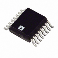
IC SENSOR TEMP QD ADC/DAC 16QSOP
Manufacturer
Analog Devices Inc
Datasheet
1.ADT7517ARQZ.pdf
(44 pages)
Specifications of ADT7517ARQZ
Function
Temp Monitoring System (Sensor)
Topology
ADC, Comparator, Multiplexer, Register Bank
Sensor Type
External & Internal
Sensing Temperature
-40°C ~ 120°C, External Sensor
Output Type
I²C™, MICROWIRE™, QSPI™, SPI™
Output Alarm
No
Output Fan
No
Voltage - Supply
2.7 V ~ 5.5 V
Operating Temperature
-40°C ~ 120°C
Mounting Type
Surface Mount
Package / Case
16-QSOP
Ic Output Type
Voltage
Sensing Accuracy Range
± 0.5°C
Supply Current
2.2mA
Supply Voltage Range
2.7V To 5.5V
Resolution (bits)
10bit
Sensor Case Style
QSOP
No. Of Pins
16
Temperature Sensor Function
Temp Sensor
Resolution
10b
Operating Temperature (min)
-40C
Operating Temperature (max)
120C
Operating Supply Voltage (min)
2.7V
Operating Supply Voltage (typ)
3.3/5V
Operating Supply Voltage (max)
5.5V
Lead Free Status / RoHS Status
Lead free / RoHS Compliant
Lead Free Status / RoHS Status
Lead free / RoHS Compliant, Lead free / RoHS Compliant
Available stocks
Company
Part Number
Manufacturer
Quantity
Price
Company:

Part Number:
ADT7517ARQZ
Manufacturer:
Analog Devices Inc
Quantity:
135


Table 18.
Bit
C0
C1
C2
C3
C4
C5
C6
C7
DAC Configuration Register (Read/Write) [Address = 0x1B]
This configuration register is an 8-bit read/write register that is
used to control the output ranges of all four DACs and also to
control the loading of the DAC registers if the LDAC pin is
disabled (Bit C3 = 1, Control Configuration 3 register).
D7
D7
0
1
Table 19.
Bit
D0
D1
D2
D3
Default settings at power-up.
1
Function
Selects between fast and slow ADC conversion speeds.
On the ADT7516 and ADT7517, this bit selects between
8-bit and 10-bit DAC output resolution on the thermal
voltage output feature. The default is 8 bits. This bit has no
effect on the ADT7519 output because this part has only
an 8-bit DAC. For the ADT7519, write 0 to this bit.
Reserved. Write 0 only.
0 = LDAC pin controls updating of DAC outputs.
1 = DAC configuration register and LDAC configuration
register control updating of DAC outputs.
Selects the ADC reference to be either internal V
for analog inputs.
Setting this bit selects DAC A voltage output to be
proportional to the internal temperature measurement.
Setting this bit selects DAC B voltage output to be
proportional to the external temperature measurement.
Reserved. Write 0 only.
0 = ADC clock at 1.4 kHz.
1 = ADC clock at 22.5 kHz. D+ and D– analog filters are
disabled.
0 = 8-bit resolution.
1 = 10-bit resolution.
0 = internal V
1 = V
D6
D6
0
1
Function
Selects the output range of DAC A.
Selects the output range of DAC B.
Selects the output range of DAC C.
Selects the output range of DAC D.
0 = 0 V to V
1 = 0 V to 2 V
0 = 0 V to V
1 = 0 V to 2 V
0 = 0 V to V
1 = 0 V to 2 V
0 = 0 V to V
1 = 0 V to 2 V
DD
.
D5
D5
0
1
REF.
REF
REF
REF
REF
D4
D4
0
REF
REF
REF
REF
.
.
.
.
1
.
.
.
.
D3
D3
0
1
D2
D2
0
1
D1
D1
0
1
REF
or V
D0
D0
0
DD
1
Rev. B | Page 33 of 44
Bit
[D4:D5]
[D6:D7]
LDAC Configuration Register (Write-Only)[Address = 0x1C]
This configuration register is an 8-bit write register that is used
to control the updating of the quad DAC outputs if the LDAC
pin is disabled and Bits[D4:D5] of the DAC configuration
register are both set to 1. Also selects either the internal or the
external V
self-clearing, that is, reading back from this register always gives
0s for these bits.
D7
D7
0
1
Table 20.
Bit
D0
D1
D2
D3
D4
D5
[D6:D7]
Interrupt Mask 1 Register (Read/Write) [Address = 0x1D]
This mask register is an 8-bit read/write register that can be
used to mask any interrupts that can cause the INT/ INT pin to
go active.
D7
D7
0
1
Default settings at power-up.
Default settings at power-up.
1
1
D6
D6
0
D6
D6
0
1
1
Function
00 = MSB write to any DAC register generates LDAC
command that updates that DAC only.
01 = MSB write to DAC B or DAC D register generates
LDAC command that updates DAC A and DAC B or
DAC C and DAC D, respectively.
10 = MSB write to DAC D register generates LDAC
command that updates all four DACs.
11 = LDAC command generated from LDAC register.
Reserved. Write 0s only.
Function
Writing a 1 to this bit generates the LDAC command
to update DAC A output only.
Writing a 1 to this bit generates the LDAC command
to update DAC B output only.
Writing a 1 to this bit generates the LDAC command
to update DAC C output only.
Writing a 1 to this bit generates the LDAC command
to update DAC D output only.
Selects either internal V
and DAC B.
Selects either internal V
and DAC D.
Reserved. Write 0s only.
REF
0 = external V
1 = internal V
0 = external V
1 = internal V
for all four DACs. Bits[D0:D3] in this register are
D5
D5
0
D5
D5
0
1
1
ADT7516/ADT7517/ADT7519
D4
D4
0
D4
D4
0
REF
REF
REF
REF
1
1
.
.
.
.
D3
D3
0
REF
REF
D3
D3
0
1
1
or external V
or external V
D2
D2
0
D2
D2
0
1
1
REF
REF
D1
0
D1
0
D1
D1
for DAC C
for DAC A
1
1
D0
D0
0
D0
D0
0
1
1
Related parts for ADT7517ARQZ
Image
Part Number
Description
Manufacturer
Datasheet
Request
R

Part Number:
Description:
±1.7g Dual-Axis IMEMS Accelerometer Evaluation Board
Manufacturer:
Analog Devices Inc
Datasheet:

Part Number:
Description:
Inertial Sensor Evaluation System
Manufacturer:
Analog Devices Inc
Datasheet:
Part Number:
Description:
Manufacturer:
Analog Devices Inc
Datasheet:
Part Number:
Description:
Manufacturer:
Analog Devices Inc
Datasheet:
Part Number:
Description:
Manufacturer:
Analog Devices Inc
Datasheet:
Part Number:
Description:
Manufacturer:
Analog Devices Inc
Datasheet:
Part Number:
Description:
Manufacturer:
Analog Devices Inc
Datasheet:
Part Number:
Description:
Manufacturer:
Analog Devices Inc
Datasheet:
Part Number:
Description:
Manufacturer:
Analog Devices Inc
Datasheet:
Part Number:
Description:
Manufacturer:
Analog Devices Inc
Datasheet:
Part Number:
Description:
Manufacturer:
Analog Devices Inc
Datasheet:
Part Number:
Description:
Manufacturer:
Analog Devices Inc
Datasheet:
Part Number:
Description:
Manufacturer:
Analog Devices Inc
Datasheet: