ADT7517ARQZ Analog Devices Inc, ADT7517ARQZ Datasheet - Page 28
ADT7517ARQZ
Manufacturer Part Number
ADT7517ARQZ
Description
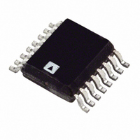
IC SENSOR TEMP QD ADC/DAC 16QSOP
Manufacturer
Analog Devices Inc
Datasheet
1.ADT7517ARQZ.pdf
(44 pages)
Specifications of ADT7517ARQZ
Function
Temp Monitoring System (Sensor)
Topology
ADC, Comparator, Multiplexer, Register Bank
Sensor Type
External & Internal
Sensing Temperature
-40°C ~ 120°C, External Sensor
Output Type
I²C™, MICROWIRE™, QSPI™, SPI™
Output Alarm
No
Output Fan
No
Voltage - Supply
2.7 V ~ 5.5 V
Operating Temperature
-40°C ~ 120°C
Mounting Type
Surface Mount
Package / Case
16-QSOP
Ic Output Type
Voltage
Sensing Accuracy Range
± 0.5°C
Supply Current
2.2mA
Supply Voltage Range
2.7V To 5.5V
Resolution (bits)
10bit
Sensor Case Style
QSOP
No. Of Pins
16
Temperature Sensor Function
Temp Sensor
Resolution
10b
Operating Temperature (min)
-40C
Operating Temperature (max)
120C
Operating Supply Voltage (min)
2.7V
Operating Supply Voltage (typ)
3.3/5V
Operating Supply Voltage (max)
5.5V
Lead Free Status / RoHS Status
Lead free / RoHS Compliant
Lead Free Status / RoHS Status
Lead free / RoHS Compliant, Lead free / RoHS Compliant
Available stocks
Company
Part Number
Manufacturer
Quantity
Price
Company:

Part Number:
ADT7517ARQZ
Manufacturer:
Analog Devices Inc
Quantity:
135


ADT7516/ADT7517/ADT7519
Table 9. Temperature Data Format
(Internal and External Temperature)
Temperature
–40°C
–25°C
–10°C
–0.25°C
0°C
+0.25°C
+10°C
+25°C
+50°C
+75°C
+100°C
+105°C
+125°C
Temperature conversion formula:
where DB9 is removed from the ADC Code in the Negative
Temperature equation.
Interrupts
The measured results from the internal temperature sensor,
external temperature sensor, V
compared with the T
T
interrupt occurs if the measurement exceeds or equals the limit
registers. These limits are stored in on-chip registers. Note that
the limit registers are 8 bits long and the conversion results are
10 bits long. If the limits are not masked, any out-of-limit
comparisons generate flags that are stored in the Interrupt
Status 1 register (Address 0x00) and Interrupt Status 2 register
(Address 0x01). One or more out-of-limit results cause the
INT/ INT output to pull either high or low depending on the
output polarity setting. It is good design practice to mask out
interrupts for channels that are of no concern to the application.
Figure 53 shows the interrupt structure for the ADT7516/
ADT7517/ADT7519. It gives a block diagram representation of
how the various measurement channels affect the INT/ INT pin.
ADT7516/ADT7517/ADT7519 REGISTERS
The ADT7516/ADT7517/ADT7519 contain registers that are
used to store the results of external and internal temperature
measurements, V
ments, high and low temperature limits, supply voltage and
analog input limits, set output DAC voltage levels, configure
multipurpose pins, and generally to control the device. A
description of these registers follows.
The register map is divided into registers of 8 bits. Each register
has its own individual address, but some consist of data that is
linked with other registers. These registers hold the 10-bit
LOW
Positive Temperature = ADC Code/4
Negative Temperature = (ADC Code – 512)/4
/V
LOW
(less than or equal to comparison) limits. An
DD
value measurements, analog input measure-
HIGH
/V
HIGH
DD
(greater than comparison) and
Digital Output
11 0110 0000
11 1001 1100
11 1101 1000
11 1111 1111
00 0000 0000
00 0000 0001
00 0010 1000
00 0110 0100
00 1100 1000
01 0010 1100
01 1001 0000
01 1010 0100
01 1111 0100
pin, and AIN inputs are
Rev. B | Page 28 of 44
conversion results of measurements taken on the temperature,
V
measurement are stored in Register Address 0x06 and the two
LSBs are stored in Register Address 0x03. These types of
registers are linked so that when the LSB register is read first,
the MSB registers associated with that LSB register are locked to
prevent any updates. To unlock these MSB registers, the user only
has to read any one of them; this has the effect of unlocking all
previously locked MSB registers. Therefore, for the preceding
example, if Register 0x03 is read first, MSB Register 0x06 and
Register 0x07 would be locked to prevent any updates to them.
If Register 0x06 is read, this register and Register 0x07 would be
subsequently unlocked.
If an MSB register is read first, its corresponding LSB register is
not locked, leaving the user with the option of just reading back
8 bits (MSB) of a 10-bit conversion result. Reading an MSB
register first does not lock other MSB registers, and likewise,
reading an LSB register first does not lock other LSB registers.
Table 10. ADT7516/ADT7517/ADT7519 Registers
R/W
Address
0x00
0x01
0x02
0x03
0x04
0x05
0x06
0x07
0x08
0x09
0x0A
0x0B
0x0C to
0x0F
0x10
0x11
0x12
0x13
DD
, and AIN channels. For example, the eight MSBs of the V
SECOND READ
FIRST READ
COMMAND
COMMAND
Name
Interrupt Status 1
Interrupt Status 2
Reserved
Internal Temp and V
External Temp and AIN1 to AIN4 LSBs
Reserved
V
Internal Temp MSBs
External Temp MSBs/AIN1 MSBs
AIN2 MSBs
AIN3 MSBs
AIN4 MSBs
Reserved
DAC A LSBs (ADT7516/ADT7517 Only)
DAC A MSBs
DAC B LSBs (ADT7516/ADT7517 Only)
DAC B MSBs
DD
MSBs
Figure 55. Phase 1 of 10-Bit Read
Figure 56. Phase 2 of 10-Bit Read
UNLOCK ASSOCIATED
LOCK ASSOCIATED
MSB REGISTERS
MSB REGISTERS
REGISTER
REGISTER
MSB
LSB
DD
LSBs
OUTPUT
OUTPUT
DATA
DATA
Power-On
Default
0x00
0x00
0x00
0x00
0x00
No default value
0x00
0x00
0x00
0x00
0x00
0x00
0x00
0x00
0x00
0x00
DD
Related parts for ADT7517ARQZ
Image
Part Number
Description
Manufacturer
Datasheet
Request
R

Part Number:
Description:
±1.7g Dual-Axis IMEMS Accelerometer Evaluation Board
Manufacturer:
Analog Devices Inc
Datasheet:

Part Number:
Description:
Inertial Sensor Evaluation System
Manufacturer:
Analog Devices Inc
Datasheet:
Part Number:
Description:
Manufacturer:
Analog Devices Inc
Datasheet:
Part Number:
Description:
Manufacturer:
Analog Devices Inc
Datasheet:
Part Number:
Description:
Manufacturer:
Analog Devices Inc
Datasheet:
Part Number:
Description:
Manufacturer:
Analog Devices Inc
Datasheet:
Part Number:
Description:
Manufacturer:
Analog Devices Inc
Datasheet:
Part Number:
Description:
Manufacturer:
Analog Devices Inc
Datasheet:
Part Number:
Description:
Manufacturer:
Analog Devices Inc
Datasheet:
Part Number:
Description:
Manufacturer:
Analog Devices Inc
Datasheet:
Part Number:
Description:
Manufacturer:
Analog Devices Inc
Datasheet:
Part Number:
Description:
Manufacturer:
Analog Devices Inc
Datasheet:
Part Number:
Description:
Manufacturer:
Analog Devices Inc
Datasheet: