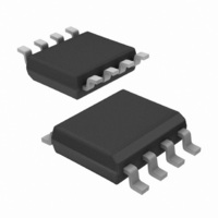
IR5001STRPBF International Rectifier, IR5001STRPBF Datasheet - Page 8

IR5001STRPBF
Manufacturer Part Number
IR5001STRPBF
Description
IC CTLR/MOSFET UNIV N-CH 8-SOIC
Manufacturer
International Rectifier
Datasheet
1.IR5001STRPBF.pdf
(12 pages)
Specifications of IR5001STRPBF
Package / Case
8-SOIC (3.9mm Width)
Mounting Type
Surface Mount
Current - Supply
500µA
Voltage - Supply
36 V ~ 75 V
Operating Temperature
0°C ~ 85°C
Applications
-48V Dist Power Systems, AdvancedTCA ® Systems
Number Of Outputs
1
Internal Switch(s)
No
Fet Type
N-Channel
Delay Time - On
27µs
Delay Time - Off
130ns
Operating Temperature (max)
125C
Operating Temperature (min)
-40C
Pin Count
8
Mounting
Surface Mount
Package Type
SOIC N
Screening Level
Automotive
Device Type
O-Ring Controller / MOSFET Driver
Input Delay
27µs
Output Delay
130ns
Driver Case Style
SOIC
No. Of Pins
8
Operating Temperature Range
0°C To +85°C
Rohs Compliant
Yes
Package
8-lead SOIC Narrow
Input Voltage
100V Max Continuous
Vline
36V to 75V 100V Max or 12Vreg
Offset Voltage (v)
-7.9mV min to 0V max
Turn-on Time (ns)
20
Turn-off Time (ns)
130
T Off Gate Drive
3A Peak
Junction Temperature
-40oC to 125oC
Special Ic
FetCheck Available
Lead Free Status / RoHS Status
Lead free / RoHS Compliant
Available stocks
Company
Part Number
Manufacturer
Quantity
Price
Part Number:
IR5001STRPBF
Manufacturer:
IR
Quantity:
20 000
DETAILED PIN DESCRIPTION
Vline and Vcc
the internal shunt regulator. The internal shunt
regulator regulates the Vcc voltage at ~12V. The
Vcc pin should always be by-passed with a ceramic
capacitor to the Gnd pin.
the IR5001S, as shown in Fig. 16. The Vline pin is
designed to bias the IR5001S directly when the
available bias voltage is above 25V and less than
100V (targeted at typical 36V – 75V telecom
applications). This connection is shown in Fig 16.a.
If the available Vbias voltage is lower than 25V, then
the IC must be biased using Vcc pin and an external
bias resistor as shown in Fig. 16.b. If the available
bias voltage is above 100V, both Vline and Vcc pins
can be used with an external bias resistor. For
calculation of the proper bias resistor value, see
example below.
www.irf.com
IR5001S, the Vbias must always be higher than the
maximum value of the Vcc UVLO threshold (10.7V).
The Rbias resistor should always be connected
between the Vbias voltage source and Vcc pin. The
Rbias resistor is selected to provide adequate Icc
current for the IC. The minimum required Icc to
guarantee proper IC operation under all conditions is
0.5mA. The maximum Icc is specified at 5mA.
Vbias
Vbias
Vline and Vcc are the input and output pins of
Both Vline and Vcc pins can be used for biasing
When the Vcc pin is used for biasing the
+
+
Rbias
Figue 16 - Biasing options for IR5001
Vline
Vcc
FETst
Vline
Vcc
FETch
FETch
FETst
IR5001
IR5001
a)
b)
OUT
Gnd
OUT
INN
INP
Gnd
INN
INP
Vbias voltages used in the example are referenced
to IR5001S Gnd:
Next, using a minimum Vcc (10.2V), verify that Icc
with the selected Rbias will be less than 5mA:
Since 2.23mA is below 5mA max Icc, the calculated
Rbias (2.6kOhm) can be used in this design.
INP and INN Inputs
speed comparator. Both pins have integrated on-
board voltage clamps and high-voltage 70kOhm
resistors.
to the source of the N-FET and INN to the drain. To
improve the noise immunity, the connections from
INN and INP pins to the source and drain terminals
of the N-FET should be as short as possible.
the state of the Vout pin of the IR5001S. When the
body diode of the Active ORing N-FET is forward-
biased and the current first starts flowing, the
voltage difference INP – INN will quickly rise toward
~700mV (typical body diode forward voltage drop).
As soon as this voltage exceeds Vhyst – Vos
(27mV typical), the Vout of the IR5001S will be
pulled high, turning the channel of the active ORing
FET on. As the channel of the N-FET becomes fully
enhanced, the (INP – INN) will reduce and stabilize
at the value determined by the source-drain current,
Isd, and Rds(on) of the N-FET:
If for some reason (due to a short-circuit failure of
the source, for example), the current reverses
direction and tries to flow from drain to source, the
(INP – INN) will become negative; The IR5001S will
then quickly pull its output low, switching the ORing
FET off. For considerations regarding the selection
of the Active ORing N-FET and R
Applications Information Section.
comparator is centered around negative 4mV, and is
always less than 0mV. This asymmetrical offset
An example of Rbias calculation is given below.
Vbias min = 12V
Vbias max = 16V
Rbias = (Vbias min – Vcc UVLOmax) / Icc min =
Icc max = (Vbias max – Vcc min)/Rbias =
INP and INN are the inputs of the internal high-
In a typical application, INP should be connected
The (INP – INN) voltage difference determines
(INP – INN) steady state = Isd * R
The offset voltage of the internal high-speed
= (12V – 10.7V) / 0.5mA = 2.6kOhm
= (16V - 10.2V) / 2.6kOhm = 2.23mA
IR5001S & (PbF)
DS(on).
DS(on)
, see
8


