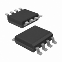
IR5001STRPBF International Rectifier, IR5001STRPBF Datasheet - Page 11

IR5001STRPBF
Manufacturer Part Number
IR5001STRPBF
Description
IC CTLR/MOSFET UNIV N-CH 8-SOIC
Manufacturer
International Rectifier
Datasheet
1.IR5001STRPBF.pdf
(12 pages)
Specifications of IR5001STRPBF
Package / Case
8-SOIC (3.9mm Width)
Mounting Type
Surface Mount
Current - Supply
500µA
Voltage - Supply
36 V ~ 75 V
Operating Temperature
0°C ~ 85°C
Applications
-48V Dist Power Systems, AdvancedTCA ® Systems
Number Of Outputs
1
Internal Switch(s)
No
Fet Type
N-Channel
Delay Time - On
27µs
Delay Time - Off
130ns
Operating Temperature (max)
125C
Operating Temperature (min)
-40C
Pin Count
8
Mounting
Surface Mount
Package Type
SOIC N
Screening Level
Automotive
Device Type
O-Ring Controller / MOSFET Driver
Input Delay
27µs
Output Delay
130ns
Driver Case Style
SOIC
No. Of Pins
8
Operating Temperature Range
0°C To +85°C
Rohs Compliant
Yes
Package
8-lead SOIC Narrow
Input Voltage
100V Max Continuous
Vline
36V to 75V 100V Max or 12Vreg
Offset Voltage (v)
-7.9mV min to 0V max
Turn-on Time (ns)
20
Turn-off Time (ns)
130
T Off Gate Drive
3A Peak
Junction Temperature
-40oC to 125oC
Special Ic
FetCheck Available
Lead Free Status / RoHS Status
Lead free / RoHS Compliant
Available stocks
Company
Part Number
Manufacturer
Quantity
Price
Part Number:
IR5001STRPBF
Manufacturer:
IR
Quantity:
20 000
www.irf.com
Rds(on) of the Active ORing FET should generate
between 50mV to 100mV of (INP – INN) voltage
during normal, steady state operation. (The normal
operation refers to current flowing from the source to
drain of the Active ORing FET, half of the full-load
system current flowing through each OR-ed source,
at nominal input voltage).
dissipation under worst-case conditions for the FET
should be calculated and verified against the data
sheet limits of the selected device.
IR5001S Thermal considerations
Maximum junction temperature of the IR5001S in an
application
operating junction temperature, specified at 125°C:
Tj = Pdiss * Rtheta j-a + Tamb <= Tj (max),
where Rtheta j-a is the thermal resistance from
junction to ambient thermal resistance (specified at
128 °C/W), Pdiss is IC power dissipation, and Tamb
is operating ambient temperature.
The maximum power dissipation can be estimated
as follows:
In a well - designed Active ORing circuit, the
should
not
exceed
Maximum
the
maximum
power
Pdiss < (Tj max – Tamb max) / Rtheta j-a
Since Tj max= 125 °C, Tamb = 85 °C, and Rtheta j-a
= 128 °C/W, the maximum power dissipation allowed
is:
Pdiss max = (125 – 85) / 128 = 0.3W
With proper selection of Icc (as discussed in the
Detailed Pin Description), the maximum power
dissipation will never be exceeded (Max Icc * Max
Vcc = 10mA * 13.9V = 0.14W).
Layout Considerations
the drain and source terminal of the Active ORing
FET. PCB trace between the Vout pin and the gate
of the N-FET should also be minimized. A minimum
of 0.1uF decoupling capacitor must be connected
from Vcc to Gnd of the IR5001S and should be
placed as close to the IR5001S as possible. Ground
should be connected to the source of N-FET
separately from the INP pin.
INN and INP should be connected very close to
IR5001S & (PbF)
11


