IR5001STRPBF International Rectifier, IR5001STRPBF Datasheet
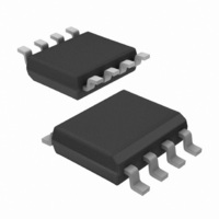
IC CTLR/MOSFET UNIV N-CH 8-SOIC

IR5001STRPBF

Manufacturer Part Number
IR5001STRPBF
Description
IC CTLR/MOSFET UNIV N-CH 8-SOIC
Manufacturer
International Rectifier
Datasheet

Specifications of IR5001STRPBF

Package / Case
8-SOIC (3.9mm Width)
Mounting Type
Surface Mount
Current - Supply
500µA
Voltage - Supply
36 V ~ 75 V
Operating Temperature
0°C ~ 85°C
Applications
-48V Dist Power Systems, AdvancedTCA ® Systems
Number Of Outputs
1
Internal Switch(s)
No
Fet Type
N-Channel
Delay Time - On
27µs
Delay Time - Off
130ns
Operating Temperature (max)
125C
Operating Temperature (min)
-40C
Pin Count
8
Mounting
Surface Mount
Package Type
SOIC N
Screening Level
Automotive
Device Type
O-Ring Controller / MOSFET Driver
Input Delay
27µs
Output Delay
130ns
Driver Case Style
SOIC
No. Of Pins
8
Operating Temperature Range
0°C To +85°C
Rohs Compliant
Yes
Package
8-lead SOIC Narrow
Input Voltage
100V Max Continuous
Vline
36V to 75V 100V Max or 12Vreg
Offset Voltage (v)
-7.9mV min to 0V max
Turn-on Time (ns)
20
Turn-off Time (ns)
130
T Off Gate Drive
3A Peak
Junction Temperature
-40oC to 125oC
Special Ic
FetCheck Available
Lead Free Status / RoHS Status
Lead free / RoHS Compliant

Available stocks

Company
Part Number
Manufacturer
Quantity
Price
Part Number:
IR5001STRPBF
Manufacturer:
IR
Quantity:
20 000
Company:
Part Number:
IR5001STRPBF
Quantity:
9 000
Company:
Part Number:
IR5001STRPBF
Quantity:
9 000
www.irf.com
DESCRIPTION
N-channel power MOSFET driver for Active ORing and
reverse polarity protection applications. The output voltage
of the IR5001S is determined based on the polarity of the
voltage difference on its input terminals. In particular, if the
current flow through an N-channel ORing FET is from
source to drain, the output of the IR5001S will be pulled
high to Vcc, thus turning the Active ORing FET on. If the
current reverses direction and flows from drain to source
(due to a short-circuit failure of the source, for example),
the IC will quickly switch the Active ORing FET off. Typical
turn-off delay for the IR5001S is only 130nS, which helps
to minimize voltage sags on the redundant dc voltage.
input contain integrated high voltage resistors and internal
clamps. This makes the IR5001S suitable for applications
at voltages up to 100V, and with a minimum number of
external components.
APPLICATIONS
FETch
FETst
Vline
Vcc
The IR5001S is a universal high-speed controller and
Both inputs to the IC (INN and INP) as well as Vline
-48V/-24V Input Active ORing for carrier
Reverse input polarity protection for
24V/48V output active ORing for
Low output voltage (12V, 5V, 3.3V...)
Active ORing of multiple voltage
1
2
3
4
JA
Top View
=128 C/W
class communication equipment
DC-DC power supplies
redundant AC-DC rectifiers
active ORing for redundant DC-DC
and AC-DC power supplies
regulators for redundant processor
power
8
7
6
5
INN
Vout
Gnd
INP
DESIG. NUMBER
PKG
S
S
F 1 - Typical application of the IR5001S in - 48V input, carrier class telecommunications equipment.
IR5001STR
IR5001S
PART
UNIVERSAL ACTIVE ORING CONTROLLER
PACKAGE / ORDERING INFORMATION
PART NUMBER COUNT PER TUBE PER REEL
IR5001STRPbF
IR5001SPbF
LEADFREE
+48V input
-48V input B
-48V input A
FET Check Pulse
FET A Status
Fet B Status
TYPICAL APPLICATION
FEATURES
A
B
Controller / driver IC in an SO-8 package for
implementation of Active ORing / reverse polarity
protection using N-channel Power MOSFETs
Suitable for both input ORing (for carrier class
telecom equipment) as well as output ORing for
redundant DC-DC and AC-DC power supplies
130ns Typical Turn-Off delay time
3A Peak Turn-Off gate drive current
Asymmetrical offset voltage of the internal high-speed
comparator prevents potential oscillations at light load
Ability to withstand continuous gate short conditions
Integrated voltage clamps on both comparator inputs
allow continuous application of up to 100V
Option to be powered either directly from 36-75V
universal telecom bus (100V max), or from an
external bias supply and bias resistor
Input/Output pins to determine the state of the Active
ORing circuit and power system redundancy
PIN
8
8
FETch
FETst
Vline
Vcc
FETch
FETst
Vline
Vcc
IR5001
IR5001
PARTS
-------
95
IR5001S & (PbF)
Vout
Vout
Gnd
Gnd
INN
INN
INP
Data Sheet No.PD60229 revB
INP
PARTS
------
2500
Oriantation
Fig A
T & R
DC
DC
1

Related parts for IR5001STRPBF

IR5001STRPBF Summary of contents

Page 1

... A B FET Check Pulse FET A Status -48V input A Fet B Status -48V input B PACKAGE / ORDERING INFORMATION LEADFREE PIN PART NUMBER COUNT PER TUBE PER REEL IR5001SPbF 8 IR5001STRPbF 8 Data Sheet No.PD60229 revB IR5001S & (PbF) IR5001 Vline Vout DC Vcc Gnd DC FETch INN FETst ...

Page 2

ABSOLUTE MAXIMUM RATINGS Vline Voltage Vcc Voltage Icc Current INN, INP Voltage FETch, FETst FETst Sink Current Junction Temperature Storage Temperature Range CAUTION: 1. Stresses above those listed in "Absolute Maximum Ratings" may cause permanent damage to the device. This ...

Page 3

PARAMETERS SYMBOL Output Section High Level Output Voltage Low Level Output Voltage Vout LO Turn-On DelayTime Rise Time Turn-Off Delay Time Fall Time FETch and FETst I(FETch) FETch Sink Current FETch Output Delay Time FETch_pd FETch Threshold Vth(FETch) FETst Threshold ...

Page 4

BLOCK DIAGRAM 50K V 1 LINE Vcc 2 12V Shunt 5V Regulator 5V, V REF 1.25V Generator 70K INP 5 clamp 70K INN 6 clamp FETch 3 Figure 2 - Simplified block diagram of the IR5001. www.irf.com UVLO 9V 5V ...

Page 5

PARAMETER DEFINITION AND TIMING DIAGRAM V OUT (0,0) V HYST V OS Figure 3 - Input Comparator Offset (Vos ) and Hysteresis Voltage (Vhyst) Definition. 10ns 90mV 50mV INP INN t d(on) ...

Page 6

TYPICAL OPERATING CHARACTERISTICS 180 170 160 150 140 130 120 -40 - Temperature (°C) Figure 6 - Turn Off Delay vs. Junction Temperature 5.7 5.6 5.5 5.4 5.3 5.2 5.1 -40 - Temperature (°C) ...

Page 7

TYPICAL OPERATING CHARACTERISTICS 13 Top: 25°C 85°C 12.8 125°C Bottom: -40°C 12.6 12.4 12.2 12 11.8 11 Vline (V) Figure 12 - Vcc vs. Vline and Junction Temperature 1.4 1.2 1 0.8 0.6 0.4 0 ...

Page 8

DETAILED PIN DESCRIPTION Vline and Vcc Vline and Vcc are the input and output pins of the internal shunt regulator. The internal shunt regulator regulates the Vcc voltage at ~12V. The Vcc pin should always be by-passed with a ceramic ...

Page 9

ORing conducting and Vout of the IR5001S is high (FET current flows from source to drain), the current must reverse the direction before the IR5001S will switch the FET off. The asymmetrical offset voltage prevents potential ...

Page 10

APPLICATION INFORMATION The IR5001S is designed for multiple active ORing and reverse polarity protection applications with minimal number of external components. Examples of typical circuit connections are shown below. Negative Rail ORing/Reverse Polarity Protection A typical connection of the IR5001S ...

Page 11

In a well - designed Active ORing circuit, the Rds(on) of the Active ORing FET should generate between 50mV to 100mV of (INP – INN) voltage during normal, steady state operation. (The normal operation refers to current flowing from the ...

Page 12

Surface Mount, Narrow Body PIN NO 8-PIN SYMBOL MIN MAX A 4.80 4.98 1.27 BSC B C 0.53 REF D 0.36 0.46 E 3.81 3.99 F 1.52 1.72 G 0.10 0.25 ...

Related keywords