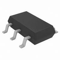
LTC4251-1IS6#TR Linear Technology, LTC4251-1IS6#TR Datasheet - Page 7

LTC4251-1IS6#TR
Manufacturer Part Number
LTC4251-1IS6#TR
Description
IC CTRLR HOTSWAP NEGVOLT SOT23-6
Manufacturer
Linear Technology
Type
Hot-Swap Controllerr
Specifications of LTC4251-1IS6#TR
Applications
General Purpose
Internal Switch(s)
No
Voltage - Supply
-36 V ~ -72 V
Operating Temperature
-40°C ~ 85°C
Mounting Type
Surface Mount
Package / Case
SOT-23-6 Thin, TSOT-23-6
Family Name
LTC4251-1
Package Type
TSOT-23
Operating Temperature (min)
-40C
Operating Temperature (max)
85C
Operating Temperature Classification
Industrial
Product Height (mm)
0.9mm
Product Length (mm)
2.9mm
Mounting
Surface Mount
Pin Count
6
Lead Free Status / RoHS Status
Contains lead / RoHS non-compliant
Lead Free Status / RoHS Status
Contains lead / RoHS non-compliant
Other names
LTC4251-1IS6TR
LTC42511IS6TR
LTC42511IS6TR
Available stocks
Company
Part Number
Manufacturer
Quantity
Price
PIN FUNCTIONS
references in the text to overvoltage, OV, V
SENSE (Pin 1): Circuit Breaker/Current Limit SENSE Pin.
Load current is monitored by sense resistor R
between SENSE and V
SENSE exceeds V
activates a 230µA TIMER pin pull-up current. The LTC4251/
LTC4251-1/LTC4251-2 latch off when C
SENSE exceeds V
amplifier pulls GATE down and regulates the MOSFET
current at V
circuit, SENSE may overshoot 100mV. If SENSE reaches
V
GATE low with a strong pull-down. To disable the circuit
breaker and current limit functions, connect SENSE to V
Kelvin-sense connections between the sense resistor and
the V
Figure 6.
V
pin to the negative side of the power supply.
V
positive side of the supply through a dropping resistor.
A shunt regulator typically clamps V
undervoltage lockout (UVLO) circuit holds GATE low until
the V
UV is high, OV is low and V
starts an initial timing cycle before initiating a GATE ramp
up. If V
immediately.
TIMER (Pin 4): Timer Input. TIMER is used to generate
a delay at start-up, and to delay shutdown in the event of
an output overload. TIMER starts an initial timing cycle
when the following conditions are met: UV is high, OV is
low, V
V
then charges C
V
pulls low and GATE is activated.
FCL
EE
IN
GATEL
TMRH
(Pin 3): Positive Supply Input. Connect this pin to the
(Pin 2): Negative Supply Voltage Input. Connect this
IN
EE
(200mV), the fast current limit comparator pulls
IN
IN
pin is greater than V
and V
(4V) the timing cycle terminates, TIMER quickly
and SENSE pins are strongly recommended, see
clears UVLO, TIMER pin is low, GATE is lower than
drops below approximately 8.2V, GATE pulls low
ACL
SENSE
T
/R
, generating a time delay. If C
CB
S
ACL
. In the event of a catastrophic short-
– V
(50mV), the circuit breaker comparator
EE
EE
(100mV), the analog current limit
, and controlled in three steps. If
< V
LKO
UV/OV refers to the UV pin for the LTC4251-2. The OV comparator in the LTC4251-2 is disabled. All
IN
CB
comes out of UVLO, TIMER
. A pull-up current of 5.8µA
(9.2V), overriding UV/OV. If
IN
OVHI
at 13V. An internal
T
charges to 4V. If
and V
T
S
charges to
OVLO
connected
do not apply to the LTC4251-2.
EE
.
If SENSE exceeds 50mV while GATE is high, a 230µA
pull-up current charges C
before TIMER reaches 4V, a 5.8µA pull-down current
slowly discharges C
integrates up to the 4V V
high with a 5.8µA pull-up source and GATE quickly pulls
low. The LTC4251/LTC4251-1/LTC4251-2 fault latches may
be cleared by either pulling TIMER low with an external
device, or by pulling UV/OV below V
UV/OV (Pin 5): Undervoltage/Overvoltage Input. This dual
function pin detects undervoltage as well as overvoltage.
The high threshold at the UV comparator is set at V
with V
comparator is set at V
OV < V
> V
LTC4251-2 attempt to start-up. The internal UVLO at V
always overrides UV/OV. A low at UV resets an internal fault
latch. A high at OV pulls GATE low but does not reset the
fault latch. A 1nF to 10nF capacitor at UV/OV eliminates
transients and switching noise from affecting the UV/OV
thresholds and prevents glitches at the GATE pin.
GATE (Pin 6): N-Channel MOSFET Gate Drive Output.
This pin is pulled high by a 58µA current source. GATE is
pulled low by invalid conditions at V
the fault latch. GATE is actively servoed to control fault
current as measured at SENSE. A compensation capacitor
at GATE stabilizes this loop. A comparator monitors GATE
to ensure that it is low before allowing an initial timing
cycle, GATE ramp up after an overvoltage event, or restart
after a current limit fault.
UVHI
UVHST
UVLO
and UV/OV < V
or UV/OV > V
hysteresis. The high threshold at the OV
LTC4251/LTC4251-1/
T
OVHI
. In the event that C
OVLO
TMRH
T
OVHI
. If SENSE drops below 50mV
with V
, the LTC4251/LTC4251-1/
, GATE pulls low. If UV/OV
threshold, TIMER latches
OVHST
LTC4251-2
IN
UVLO
(UVLO), UV/OV, or
hysteresis. If UV/
.
T
eventually
415112fb
UVHI
7
IN


