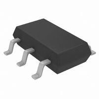
LTC4251-1IS6#TR Linear Technology, LTC4251-1IS6#TR Datasheet - Page 11

LTC4251-1IS6#TR
Manufacturer Part Number
LTC4251-1IS6#TR
Description
IC CTRLR HOTSWAP NEGVOLT SOT23-6
Manufacturer
Linear Technology
Type
Hot-Swap Controllerr
Specifications of LTC4251-1IS6#TR
Applications
General Purpose
Internal Switch(s)
No
Voltage - Supply
-36 V ~ -72 V
Operating Temperature
-40°C ~ 85°C
Mounting Type
Surface Mount
Package / Case
SOT-23-6 Thin, TSOT-23-6
Family Name
LTC4251-1
Package Type
TSOT-23
Operating Temperature (min)
-40C
Operating Temperature (max)
85C
Operating Temperature Classification
Industrial
Product Height (mm)
0.9mm
Product Length (mm)
2.9mm
Mounting
Surface Mount
Pin Count
6
Lead Free Status / RoHS Status
Contains lead / RoHS non-compliant
Lead Free Status / RoHS Status
Contains lead / RoHS non-compliant
Other names
LTC4251-1IS6TR
LTC42511IS6TR
LTC42511IS6TR
Available stocks
Company
Part Number
Manufacturer
Quantity
Price
APPLICATIONS INFORMATION
SHUNT REGULATOR
A fast responding shunt regulator clamps the V
13V (V
current limiting resistor, R
C
at start-up.
To meet creepage requirements R
or more series connected units, such as two 5.1k or three
3.3k resistors. This introduces a wider total spacing than is
possible with a single component while at the same time
ballasting the potential across the gap under each resistor.
The LTC4251 is fundamentally a low voltage device that
operates with –48V as its reference ground. To further
protect against arc discharge into its pins, the area in and
around the LTC4251 and all associated components should
be free of any other planes such as chassis ground, return,
or secondary-side power and ground planes.
V
package, and is tested to survive a 100µs, 100mA pulse. To
protect V
clamp V
V
Kelvin terminal as illustrated in Figure 2, keeping trace
lengths between V
INTERNAL UNDERVOLTAGE LOCKOUT (UVLO)
Internal circuitry monitors V
thresholds are defined by V
When V
below 8.2V (V
low. The UVLO function at V
the UV/OV pin. These are completely separate functions.
UV/OV COMPARATORS
Two hysteretic comparators for detecting under- and
overvoltage conditions, with the following thresholds,
monitor the dual function UV/OV pin:
UV turning on at V
UV turning off at V
IN
IN
EE
filters supply transients and contributes a short delay
is rated handle 30mA within the thermal limits of the
and all V
Z
). Power is derived from –48RTN by an external
IN
IN
IN
rises above 9.2V (V
to V
against damage from higher amplitude spikes,
EE
LKO
referred components to the sense resistor
EE
-V
IN
with a 13V Zener diode. Star connect
UVHI
UVLO
, C
LKH
IN
) it is disabled and GATE is pulled
, D
IN
IN
IN
IN
. A 1µF decoupling capacitor,
LKO
and V
should not be confused with
for undervoltage. The exact
LKO
and its hysteresis, V
IN
EE
) the chip is enabled;
may be split into two
as short as possible.
IN
pin to
LKH
.
OV turning off at V
OV turning on at V
The UV and OV trip point ratio for LTC4251 is designed to
match the standard telecom operating range of 43V to 75V.
The LTC4251-2 implements a UV threshold of 43V only.
A divider (R1, R2) is used to scale the supply voltage. Using
R1 = 402k and R2 = 32.4k gives a typical operating range
of 43.2V to 74.4V. The under- and overvoltage shutdown
thresholds are then 39.2V and 82.5V. 1% divider resis-
tors are recommended to preserve threshold accuracy.
The same resistor values can be used for the LTC4251-2.
The R1-R2 divider values shown in the Typical Application
set a standing current of slightly more than 100µA, and
define an impedance at UV/OV of 30k. In most applications,
30k impedance coupled with 300mV UV hysteresis makes
the LTC4251/LTC4251-1/LTC4251-2 insensitive to noise. If
more noise immunity is desired, add a 1nF to 10nF filter
capacitor from UV/OV to V
The UV and OV trip point thresholds for the LTC4251-1 are
designed to encompass the standard telecom operating
range of –36V to –72V.
A divider (R1, R2) is used to scale the supply voltage.
Using R1 = 442k and R2 = 34.8k gives a typical operating
range of 33.2V to 81V. The typical under- and overvoltage
shutdown thresholds are then 29.6V and 84.5V. 1% divider
resistors are recommended to preserve threshold accuracy.
The R1-R2 divider values shown in the Typical Application
set a standing current of slightly more than 100µA, and
define an impedance at UV/OV of 32k. In most applica-
tions, 32k impedance coupled with 260mV UV hysteresis
makes the LTC4251-1 insensitive to noise. If more noise
immunity is desired, add a 1nF to 10nF filter capacitor
from UV/OV to V
UV/OV OPERATION
A low input to the UV comparator will reset the chip and
pull the GATE and TIMER pins low. A low-to-high UV
transition will initiate an initial timing sequence if the three
remaining interlock conditions are met.
LTC4251/LTC4251-1/
EE
OVLO
OVHI
.
EE
.
LTC4251-2
11
415112fb


