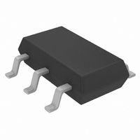
LTC4251-1IS6#TR Linear Technology, LTC4251-1IS6#TR Datasheet - Page 15

LTC4251-1IS6#TR
Manufacturer Part Number
LTC4251-1IS6#TR
Description
IC CTRLR HOTSWAP NEGVOLT SOT23-6
Manufacturer
Linear Technology
Type
Hot-Swap Controllerr
Specifications of LTC4251-1IS6#TR
Applications
General Purpose
Internal Switch(s)
No
Voltage - Supply
-36 V ~ -72 V
Operating Temperature
-40°C ~ 85°C
Mounting Type
Surface Mount
Package / Case
SOT-23-6 Thin, TSOT-23-6
Family Name
LTC4251-1
Package Type
TSOT-23
Operating Temperature (min)
-40C
Operating Temperature (max)
85C
Operating Temperature Classification
Industrial
Product Height (mm)
0.9mm
Product Length (mm)
2.9mm
Mounting
Surface Mount
Pin Count
6
Lead Free Status / RoHS Status
Contains lead / RoHS non-compliant
Lead Free Status / RoHS Status
Contains lead / RoHS non-compliant
Other names
LTC4251-1IS6TR
LTC42511IS6TR
LTC42511IS6TR
Available stocks
Company
Part Number
Manufacturer
Quantity
Price
APPLICATIONS INFORMATION
FREQUENCY COMPENSATION
The LTC4251/LTC4251-1/LTC4251-2 typical frequency
compensation network for the analog current limit loop
is a series R
depicts the relationship between the compensation ca-
pacitor C
is used to select a starting value for C
MOSFET’s C
shown for several popular MOSFETs. Differences in the
optimized value of C
Nevertheless, compensation values should be verified by
board level short-circuit testing.
As seen in Figure 4 previously, at the onset of a short-
circuit event, the input supply voltage can ring dramatically
owing to series inductance. If this voltage avalanches the
MOSFET, current continues to flow through the MOSFET
to the output. The analog current limit loop cannot control
this current flow and therefore the loop undershoots. This
effect cannot be eliminated by frequency compensation. A
zener diode is required to clamp the input supply voltage
and prevent MOSFET avalanche.
SENSE RESISTOR CONSIDERATIONS
For proper circuit breaker operation, Kelvin-sense PCB
connections between the sense resistor and the V
SENSE pins are strongly recommended. The drawing in
Figure 6 illustrates the correct way of making connections
between the LTC4251/LTC4251-1/LTC4251-2 and the sense
C
Figure 5. Recommended Compensation
Capacitor C
and the MOSFET’s C
60
50
40
30
20
10
ISS
0
C
0
IRF530
(10Ω) and C
specification. Optimized values for C
IRF740
IRF540
2000
C
C
IRF3710
vs MOSFET C
versus the starting value are small.
MOSFET C
4000
C
connected to V
ISS
(pF)
ISS
ISS
MTY100N10E
6000
. The line in Figure 5
C
425112 F05
based upon the
8000
EE
. Figure 5
EE
C
and
are
resistor. PCB layout should be balanced and symmetrical to
minimize wiring errors. In addition, the PCB layout for the
sense resistor should include good thermal management
techniques for optimal sense resistor power dissipation.
TIMING WAVEFORMS
System Power-Up
Figure 7 details the timing waveforms for a typical
power-up sequence in the case where a board is already
installed in the backplane and system power is applied
abruptly. At time point 1, the supply ramps up, together
with UV/OV and V
by the V
V
V
When all conditions are met, an initial timing cycle starts
and the TIMER capacitor is charged by a 5.8µA current
source pull-up. At time point 3, TIMER reaches the V
threshold and the initial timing cycle terminates. The
TIMER capacitor is then quickly discharged. At time point
4, the V
GATE < V
a start-up cycle is allowed to begin. GATE sources 58µA
into the external MOSFET gate and compensation network.
When the GATE voltage reaches the MOSFET’s threshold,
current begins flowing into the load capacitor. At time
point 5, the SENSE voltage (V
threshold and activates the TIMER. The TIMER capacitor
TRACK WIDTH W:
LKO
OVLO
ON 1 OZ COPPER
0.03" PER AMP
Figure 6. Making PCB Connections to the Sense Resistor
and the internal logic checks for V
, TIMER < V
TMRL
IN
GATEL
CURRENT FLOW
bypass capacitor. At time point 2, V
FROM LOAD
threshold is reached and the conditions of
LTC4251/LTC4251-1/
W
and SENSE < V
TMRL
OUT
. V
, GATE < V
SENSE
IN
SENSE RESISTOR
TO
follows at a slower rate as set
SENSE
CB
must be satisfied before
GATEL
V
TO
– V
EE
LTC4251-2
EE
TO –48V BACKPLANE
and SENSE < V
) reaches the V
CURRENT FLOW
UVHI
< UV/OV <
IN
exceeds
15
425112 F06
415112fb
TMRH
CB
CB
.


