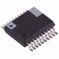
ADE7763ARSRL Analog Devices Inc, ADE7763ARSRL Datasheet - Page 22

ADE7763ARSRL
Manufacturer Part Number
ADE7763ARSRL
Description
IC ENERGY METER 1PHASE 20SSOP
Manufacturer
Analog Devices Inc
Datasheet
1.ADE7763ARSZRL.pdf
(56 pages)
Specifications of ADE7763ARSRL
Input Impedance
390 KOhm
Measurement Error
0.1%
Voltage - I/o High
2.4V
Voltage - I/o Low
0.8V
Current - Supply
3mA
Voltage - Supply
4.75 V ~ 5.25 V
Operating Temperature
-40°C ~ 85°C
Mounting Type
Surface Mount
Package / Case
20-SSOP (0.200", 5.30mm Width)
Meter Type
Single Phase
For Use With
EVAL-ADE7763ZEB - BOARD EVALUATION FOR ADE7763
Lead Free Status / RoHS Status
Contains lead / RoHS non-compliant
ADE7763
With the specified full-scale analog input signal of 0.5 V, the ADC
produces an output code that is approximately ±2,642,412d—
see the Channel 1 ADC section. The equivalent rms value of a
full-scale ac signal is 1,868,467d (0x1C82B3). The current rms
measurement provided in the ADE7763 is accurate to within
0.5% for signal input between full scale and full scale/100.
Converting the register value to its equivalent in amps must be
done externally in the microprocessor using an amps/LSB
constant. To minimize noise, synchronize the reading of the
rms register with the zero crossing of the voltage input and take
the average of a number of readings.
Channel 1 RMS Offset Compensation
The ADE7763 incorporates a Channel 1 rms offset compensa-
tion register (IRMSOS). This is a 12-bit, signed register that can
be used to remove offset in the Channel 1 rms calculation. An
offset might exist in the rms calculation due to input noises that
are integrated in the dc component of V
tion eliminates the influence of input noises from the rms
measurement.
One LSB of the Channel 1 rms offset is equivalent to 32,768 LSB
of the square of the Channel 1 rms register. Assuming that the
maximum value from the Channel 1 rms calculation is
1,868,467d with full-scale ac inputs, then 1 LSB of the Channel 1
rms offset represents 0.46% of the measurement error at –60 dB
down of full scale.
where IRMS
To measure the offset of the rms measurement, two data points
are needed from nonzero input values, for example, the base
current, I
measurements.
CHANNEL 2 ADC
Channel 2 Sampling
In Channel 2 waveform sampling mode (MODE[14:13] = 1, 1
and WSMP = 1), the ADC output code scaling for Channel 2 is
not the same as it is for Channel 1. The Channel 2 waveform
IRMS =
b
, and I
0
is the rms measurement without offset correction.
IRMS
max
/100. The offset can be calculated from these
0
2
+ IRMSOS
0xD7 AE14
0x28 51EC
CHANNEL 1
CURRENT SIGNAL (i(t))
0x00
×
32768
2
(t). The offset calibra-
HPF1
24
Figure 45. Channel 1 RMS Signal Processing
Rev. B | Page 22 of 56
(4)
LPF3
sgn
2
25
sample is a 16-bit word and sign extended to 24 bits. For normal
operation, the differential voltage signal between V2P and V2N
should not exceed 0.5 V. With maximum voltage input (±0.5 V
at PGA gain of 1), the output from the ADC swings between
0x2852 and 0xD7AE (±10,322d). However, before being passed
to the waveform register, the ADC output is passed through a
single-pole, low-pass filter with a cutoff frequency of 140 Hz.
The plots in Figure 46 show the magnitude and phase response
of this filter.
The LPF1 has the effect of attenuating the signal. For example,
if the line frequency is 60 Hz, the signal at the output of LPF1
will be attenuated by about 8%.
Note LPF1 does not affect the active power calculation. The
signal processing chain in Channel 2 is illustrated in Figure 47.
2
26
IRMSOS[11:0]
2
27
–10
–20
–30
–40
–50
–60
–70
–80
–90
| H ( f )| =
+
0
10
1
2
17
50Hz, –19.7°
Figure 46. Magnitude and Phase Response of LPF1
2
16
1
2
60Hz, –23.2°
+
15
⎛
⎜
⎜
⎝
0x1C 82B3
140
60
50Hz, –0.52dB
24
1
Hz
0x00
Hz
IRMS(t)
FREQUENCY (Hz)
⎞
⎟
⎟
⎠
IRMS
2
= 0.919 = −0.73 db
10
2
60Hz, –0.73dB
10
3
–2
–4
–6
–8
–10
–12
–14
–16
–18
0
(5)


