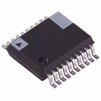
ADE7763ARSZ Analog Devices Inc, ADE7763ARSZ Datasheet - Page 31

ADE7763ARSZ
Manufacturer Part Number
ADE7763ARSZ
Description
IC ENERGY METERING 1PHASE 20SSOP
Manufacturer
Analog Devices Inc
Datasheet
1.ADE7763ARSZRL.pdf
(56 pages)
Specifications of ADE7763ARSZ
Input Impedance
390 KOhm
Measurement Error
0.1%
Voltage - I/o High
2.4V
Voltage - I/o Low
0.8V
Current - Supply
3mA
Voltage - Supply
4.75 V ~ 5.25 V
Operating Temperature
-40°C ~ 85°C
Mounting Type
Surface Mount
Package / Case
20-SSOP (0.200", 5.30mm Width)
Meter Type
Single Phase
Ic Function
Single-Phase Active And Apparent Energy Metering IC
Supply Voltage Range
4.75V To 5.25V
Operating Temperature Range
-40°C To +85°C
Digital Ic Case Style
SSOP
No. Of Pins
20
Lead Free Status / RoHS Status
Lead free / RoHS Compliant
For Use With
EVAL-ADE7763ZEB - BOARD EVALUATION FOR ADE7763
Lead Free Status / RoHS Status
Lead free / RoHS Compliant, Lead free / RoHS Compliant
Available stocks
Company
Part Number
Manufacturer
Quantity
Price
Part Number:
ADE7763ARSZ
Manufacturer:
ADI/亚德诺
Quantity:
20 000
Part Number:
ADE7763ARSZRL
Manufacturer:
ADI/亚德诺
Quantity:
20 000
APPARENT POWER CALCULATION
The apparent power is the maximum power that can be
delivered to a load. V
current delivered to the load; the apparent power (AP) is
defined as V
the apparent power generally represents the phase shift due to
nonresistive loads. For single-phase applications, θ represents
the angle between the voltage and the current signals—see
Figure 63. Equation 24 gives an expression of the instantaneous
power signal in an ac system with a phase shift.
The apparent power is defined as V
independent from the phase angle between the current and
the voltage.
Figure 64 illustrates the signal processing in each phase for the
calculation of the apparent power in the ADE7763.
V
I
RMS
RMS
CURRENT RMS SIGNAL – i(t)
v t
i t
p
p
( )
0x1C 82B3
( )
VOLTAGE RMS SIGNAL– v(t)
0x17 D338
(
(
t
t
)
)
=
=
0x00
0x00
=
=
REACTIVE
V
v
rms
2
2
POWER
(
rms
Figure 64. Apparent Power Signal Processing
I
t
V
rms
)
× I
rms
×
I
sin(
t i
rms
rms
sin( )
(
. The angle θ between the active power and
)
rms
ω
Figure 63. Power Triangle
cos(
ω
t
and I
t
+
θ
θ
)
)
θ
−
rms
MULTIPLIER
V
are the effective voltage and
rms
APPARENT POWER
rms
I
ACTIVE POWER
rms
× I
VAGAIN
cos(
rms
. This expression is
2
0xA D055
ω
t
APPARENT POWER
+
θ
SIGNAL (P)
)
(23)
(24)
Rev. B | Page 31 of 56
The gain of the apparent energy can be adjusted by using the
multiplier and VAGAIN register (VAGAIN[11:0]). The gain is
adjusted by writing a twos complement, 12-bit word to the
VAGAIN register. Equation 25 shows how the gain adjustment
is related to the contents of the VAGAIN register.
For example, when 0x7FF is written to the VAGAIN register, the
power output is scaled up by 50%. 0x7FF = 2047d, 2047/2
Similarly, 0x800 = –2047d (signed, twos complement) and power
output is scaled by –50%. Each LSB represents 0.0244% of the
power output. The apparent power is calculated with the current
and voltage rms values obtained in the rms blocks of the
ADE7763. Figure 65 shows the maximum code (hexadecimal)
output range of the apparent power signal. Note that the output
range changes depending on the contents of the apparent power
gain registers. The minimum output range is given when the
apparent power gain register content is equal to 0x800; the
maximum range is given by writing 0x7FF to the apparent
power gain register. This can be used to calibrate the apparent
power (or energy) calculation in the ADE7763.
Apparent Power Offset Calibration
Each rms measurement includes an offset compensation
register to calibrate and eliminate the dc component in the rms
value—see the Channel 1 RMS Calculation and Channel 2 RMS
Calculation sections. The Channel 1 and Channel 2 rms values
are then multiplied together in the apparent power signal
processing. Because no additional offsets are created in the
multiplication of the rms values, there is no specific offset
compensation in the apparent power signal processing. The
offset compensation of the apparent power measurement is
done by calibrating each individual rms measurement.
OutputVAGA
Figure 65. Apparent Power Calculation Output Range
0x10 3880
0xA D055
0x5 682B
0x0 0000
APPARENT POWER 100% FS
IN
CHANNEL INPUTS: 0.5V/GAIN
VOLTAGE AND CURRENT
0x000
CALIBRATION RANGE,
=
APPARENT POWER
⎛
⎜ ⎜
⎝
{VAGAIN[11:0]}
Apparent
APPARENT POWER 150% FS
0x7FF
APPARENT POWER 50% FS
Power
0x800
×
⎧
⎨
⎩
1
+
VAGAIN
ADE7763
2
12
12
= 0.5.
⎫
⎬
⎭
⎞
⎟ ⎟
⎠
(25)


