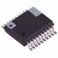
ADE7763ARSZ Analog Devices Inc, ADE7763ARSZ Datasheet - Page 20

ADE7763ARSZ
Manufacturer Part Number
ADE7763ARSZ
Description
IC ENERGY METERING 1PHASE 20SSOP
Manufacturer
Analog Devices Inc
Datasheet
1.ADE7763ARSZRL.pdf
(56 pages)
Specifications of ADE7763ARSZ
Input Impedance
390 KOhm
Measurement Error
0.1%
Voltage - I/o High
2.4V
Voltage - I/o Low
0.8V
Current - Supply
3mA
Voltage - Supply
4.75 V ~ 5.25 V
Operating Temperature
-40°C ~ 85°C
Mounting Type
Surface Mount
Package / Case
20-SSOP (0.200", 5.30mm Width)
Meter Type
Single Phase
Ic Function
Single-Phase Active And Apparent Energy Metering IC
Supply Voltage Range
4.75V To 5.25V
Operating Temperature Range
-40°C To +85°C
Digital Ic Case Style
SSOP
No. Of Pins
20
Lead Free Status / RoHS Status
Lead free / RoHS Compliant
For Use With
EVAL-ADE7763ZEB - BOARD EVALUATION FOR ADE7763
Lead Free Status / RoHS Status
Lead free / RoHS Compliant, Lead free / RoHS Compliant
Available stocks
Company
Part Number
Manufacturer
Quantity
Price
Part Number:
ADE7763ARSZ
Manufacturer:
ADI/亚德诺
Quantity:
20 000
Part Number:
ADE7763ARSZRL
Manufacturer:
ADI/亚德诺
Quantity:
20 000
ADE7763
Antialias Filter
Figure 39 also shows an analog low-pass filter (RC) on the input
to the modulator. This filter prevents aliasing, which is an
artifact of all sampled systems. Aliasing means that frequency
components in the input signal to the ADC that are higher than
half the sampling rate of the ADC appear in the sampled signal
at a frequency below half the sampling rate. Figure 41 illustrates
the effect. Frequency components (shown as arrows) above half
the sampling frequency (also known as the Nyquist frequency,
i.e., 447 kHz) are imaged or folded back down below 447 kHz.
This happens with all ADCs, regardless of the architecture. In
the example shown, only frequencies near the sampling
frequency, i.e., 894 kHz, move into the band of interest for
metering, i.e., 40 Hz to 2 kHz. This allows the use of a very
simple LPF (low-pass filter) to attenuate high frequency (near
900 kHz) noise, and it prevents distortion in the band of interest.
For conventional current sensors, a simple RC filter (single-pole
LPF) with a corner frequency of 10 kHz produces an attenuation
of approximately 40 dB at 894 kHz—see Figure 41. The 20 dB
per decade attenuation is usually sufficient to eliminate the effects
of aliasing for conventional current sensors; however, for a di/dt
sensor such as a Rogowski coil, the sensor has a 20 dB per decade
gain. This neutralizes the –20 dB per decade attenuation
produced by one simple LPF. Therefore, when using a di/dt
sensor, care should be taken to offset the 20 dB per decade gain.
One simple approach is to cascade two RC filters to produce the
–40 dB per decade attenuation.
ADC Transfer Function
The following expression relates the output of the LPF in the
Σ -Δ ADC to the analog input signal level. Both ADCs in the
ADE7763 are designed to produce the same output code for the
same input signal level.
Therefore, with a full-scale signal on the input of 0.5 V and an
internal reference of 2.42 V, the ADC output code is nominally
165,151, or 0x2851F. The maximum code from the ADC is
±262,144; this is equivalent to an input signal level of ±0.794 V.
However, for specified performance, do not exceed the 0.5 V
full-scale input signal level.
0
Figure 41. ADC and Signal Processing in Channel 1 Outline Dimensions
Code ADC
2
FREQUENCIES
IMAGE
(
) 3.0492
=
FREQUENCY (kHz)
ALIASING EFFECTS
447
×
V
V
OUT
IN
×
262,144
894
FREQUENCY
SAMPLING
Rev. B | Page 20 of 56
(1)
Reference Circuit
Figure 42 shows a simplified version of the reference output
circuitry. The nominal reference voltage at the REF
2.42 V. This is the reference voltage used for the ADCs. However,
Channel 1 has three input range options that are selected by
dividing down the reference value used for the ADC in
Channel 1. The reference value used for Channel 1 is divided
down to ½ and ¼ of the nominal value by using an internal
resistor divider, as shown in Figure 42.
The REF
a 2.5 V reference. Note that the nominal reference value supplied
to the ADCs is now 2.5 V, not 2.42 V, which increases the
nominal analog input signal range by 2.5/2.42 × 100% = 3% or
from 0.5 V to 0.5165 V.
The voltage of the ADE7763 reference drifts slightly with changes
in temperature—see Table 1 for the temperature coefficient
specification (in ppm/°C). The value of the temperature drift
varies from part to part. Because the reference is used for the
ADCs in both Channels 1 and 2, any x% drift in the reference
results in 2x% deviation in the meter accuracy. The reference
drift that results from a temperature change is usually very
small, typically much smaller than the drift of other components
on a meter. However, if guaranteed temperature performance is
needed, use an external voltage reference. Alternatively, the
meter can be calibrated at multiple temperatures. Real-time
compensation can be achieved easily by using the on-chip
temperature sensor.
CHANNEL 1 ADC
Figure 43 shows the ADC and signal processing chain for
Channel 1. In waveform sampling mode, the ADC outputs a
signed, twos complement, 24-bit data-word at a maximum of
27.9 kSPS (CLKIN/128). With the specified full-scale analog
input signal of 0.5 V (or 0.25 V or 0.125 V—see the Analog
Inputs section), the ADC produces an output code that is
approximately between 0x28 51EC (+2,642,412d) and
0xD7 AE14 (–2,642,412d)—see Figure 43.
PTAT
IN/OUT
60μA
pin can be overdriven by an external source such as
2.5V
LOAD = 10μA
Figure 42. Reference Circuit Output
MAXIMUM
1.7kΩ
12.5kΩ
12.5kΩ
12.5kΩ
12.5kΩ
REF
2.42V
IN/OUT
OUTPUT
IMPEDANCE
6kΩ
REFERENCE INPUT
TO ADC CHANNEL 1
(RANGE SELECT)
2.42V, 1.21V, 0.6V
IN/OUT
pin is


