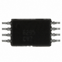
ISL6295CVZ Intersil, ISL6295CVZ Datasheet - Page 6

ISL6295CVZ
Manufacturer Part Number
ISL6295CVZ
Description
IC FUEL GAUGE LOW VOLTAGE8-TSSOP
Manufacturer
Intersil
Datasheet
1.ISL6295CVZ.pdf
(25 pages)
Specifications of ISL6295CVZ
Function
Fuel, Gas Gauge/Monitor
Battery Type
Lithium-Ion (Li-Ion), Lithium-Polymer (Li-Pol)
Voltage - Supply
2.8 V ~ 7 V
Operating Temperature
-20°C ~ 85°C
Mounting Type
Surface Mount
Package / Case
8-TSSOP
Battery Management Function
Fuel Gauge
Supply Voltage Range
2.8V To 7V
Interface Type
2-Wire, Serial, I2C
Battery Ic Case Style
TSSOP
No. Of Pins
8
Rohs Compliant
Yes
Lead Free Status / RoHS Status
Lead free / RoHS Compliant
Available stocks
Company
Part Number
Manufacturer
Quantity
Price
Company:
Part Number:
ISL6295CVZ
Manufacturer:
Intersil
Quantity:
40
Company:
Part Number:
ISL6295CVZ
Manufacturer:
INTERSIL
Quantity:
17
Part Number:
ISL6295CVZ
Manufacturer:
INTERSIL
Quantity:
20 000
the user through 8 A/D control registers. These registers
determine the input source, conversion resolution, reference
voltage, and sequence of conversions during an A/D
conversion cycle. During the cycle, the A/D logic accesses
each register in sequence and performs the conversion
specified by the bits within the registers. Each register
contains an enable bit, a resolution field, a select bit for
single-ended (340mV reference) or differential (170mV
reference) conversion, and a select field for the analog input
multiplexer. The result from each conversion is stored in one
of eight corresponding 16-bit result registers.
If the “Enable” bit is set within a control register, a conversion
will be performed. If it is disabled, that conversion will be
skipped and the logic will move on to the next register. In this
manner, the user can specify a sequence of conversions that
will be performed during each A/D cycle.
As stated above, the input source for each of the registers is
programmable. The 3-bit MUX field within each control
register selects one of seven possible input sources for the
A/D conversion. The list of input sources is as follows:
• Charge/discharge Current (Voltage from SR pin to GND)
• Internal temperature sensor
• External thermistor (Constant current source on NTC pin)
• Battery pack voltage
• Reserved
• General purpose A/D voltage
• ADC offset (Conversion performed with ADC input
However, the accumulator/timer functions are “hard-wired” to
specific A/D result registers. For this reason, the control/
result registers are given names which indicate their primary
intended usage:
REGISTER
internally shorted to ground) to determine offset error
associated with the converter
A/D
0
1
2
3
4
5
6
7
REGISTER
CONTROL
Reserved
GPADctrl
OFFSctrl
AUXctrl
VPctrl
ETctrl
ITctrl
Ictrl
REGISTER
GPADres General Purpose A/D Input
RESULT
OFFSres Internal ADC offset voltage
AUXres
ETres
VPres
ITres
Ires
6
Any
Battery Pack Current
(via sense resistor)
Internal Temperature Sensor
External Temperature
Sensor
Battery Pack Voltage
(with input grounded)
INPUT SOURCE
INTENDED
ISL6295
The 3-bit “resolution” field in each A/D control register
determines the magnitude resolution of the conversion, from
a minimum of 8-bits to a maximum of 15-bits. The time
required to complete the conversion is a function of the
number of bits of resolution selected. The conversion time
can be calculated as follows:
T
where “N” is the number of bits of magnitude resolution
selected
The “Ref” bit selects either a differential or single-ended
conversion. For differential conversions, the 170mV
reference is used. For single-ended conversion the 340mV
reference is selected. Single-ended conversions would be
used for measurements of pack voltage while a differential
conversion is required for current measurement.
The value of the LSB in the result register is as follows:
For single-ended conversion,
A/D LSB = 340 mV/2
For differential conversion,
A/D LSB = 170 mV/2
For both differential and single-ended conversions, the result
value is given in sign-magnitude format (i.e. a sign bit and 15
magnitude bits). When N less than 15 is selected, the
conversion result is padded with trailing zeroes. Note that
the single-ended reference should not be used for a
negative measurement. Though the sign-magnitude value
presented may still look valid, the accumulator will not be
able to interpret the result for proper accumulation.
CURRENT MEASUREMENT
Charge and discharge currents are measured using a 5 to
600mΩ sense resistor that is connected between the SR and
GND pins. The sense resistor value chosen must
accommodate the system’s lowest and highest expected
charge and discharge currents, including suspend and
standby currents, while maintaining a voltage of no more
than +152mV presented at the SR pin.
In order to perform charge and discharge current
measurements, the Ictrl register must be programmed with
the SR pin as the analog input source. If charge and
discharge accumulation is desired, the Ictrl and
corresponding Ires registers should be used to select current
measurement since the DCA, DTC, CCA, and CTC registers
are updated by the measurement results from the Ires
register.
When a 20mΩ sense resistor is used, the value of the LSB in
units of current is:
5.19µV/20mΩ = 259.5µA
ADC
15
S
= 30.52µs * 2
14
(N+1)
15
15
Magnitude
= 10.38µV
= 5.19µV
0
February 8, 2011
FN9074.2


