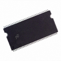
MT46V16M16P-75:F Micron Technology Inc, MT46V16M16P-75:F Datasheet - Page 78

MT46V16M16P-75:F
Manufacturer Part Number
MT46V16M16P-75:F
Description
IC DDR SDRAM 256MBIT 66TSOP
Manufacturer
Micron Technology Inc
Type
DDR SDRAMr
Datasheet
1.MT46V16M16CY-5BK_TR.pdf
(93 pages)
Specifications of MT46V16M16P-75:F
Format - Memory
RAM
Memory Type
DDR SDRAM
Memory Size
256M (16Mx16)
Speed
7.5ns
Interface
Parallel
Voltage - Supply
2.3 V ~ 2.7 V
Operating Temperature
0°C ~ 70°C
Package / Case
66-TSOP
Organization
16Mx16
Density
256Mb
Address Bus
15b
Access Time (max)
750ps
Maximum Clock Rate
266MHz
Operating Supply Voltage (typ)
2.5V
Package Type
TSOP
Operating Temp Range
0C to 70C
Operating Supply Voltage (max)
2.7V
Operating Supply Voltage (min)
2.3V
Supply Current
185mA
Pin Count
66
Mounting
Surface Mount
Operating Temperature Classification
Commercial
Lead Free Status / RoHS Status
Lead free / RoHS Compliant
Figure 40:
Figure 41:
PDF: 09005aef80768abb/Source: 09005aef82a95a3a
DDR_x4x8x16_Core2.fm - 256Mb DDR: Rev. O, Core DDR: Rev. B 1/09 EN
Nonconsecutive WRITE-to-WRITE
Random WRITE Cycles
Notes:
Notes:
t DQSS (NOM)
1. DI b (or n) = data-in from column b (or column n).
2. Three subsequent elements of data-in are applied in the programmed order following DI b.
3. Three subsequent elements of data-in are applied in the programmed order following DI n.
4. An uninterrupted burst of 4 is shown.
5. Each WRITE command may be to any bank.
Command
1. DI b (or x or n or a or g) = data-in from column b (or column x, or column n, or column a, or
2. b', x', n', a' or g' indicate the next data-in following DO b, DO x, DO n, DO a, or DO g,
3. Programmed BL = 2, BL = 4, or BL = 8 in cases shown.
4. Each WRITE command may be to any bank.
Address
Command
column g).
respectively.
Address
DQS
CK#
DM
DQ
CK
DQS
CK#
DM
DQ
CK
WRITE
Bank,
Col b
T0
WRITE
Bank,
Col b
T0
t DQSS (NOM)
t DQSS
WRITE
Bank,
Col x
DI
T1
b
NOP
DI
T1
b
76
T1n
DI
b'
T1n
WRITE
Bank,
Col n
Micron Technology, Inc., reserves the right to change products or specifications without notice.
T2
DI
x
NOP
T2
T2n
DI
x'
T2n
256Mb: x4, x8, x16 DDR SDRAM
WRITE
Bank,
Col a
T3
DI
n
WRITE
Bank,
Col n
T3
Transitioning Data
T3n
DI
n'
Transitioning Data
©2003 Micron Technology, Inc. All rights reserved.
WRITE
Bank,
Col g
T4
DI
a
NOP
DI
T4
n
T4n
DI
a'
T4n
Operations
NOP
T5
DI
g
Don’t Care
T5
NOP
Don’t Care
T5n
DI
g'
T5n


