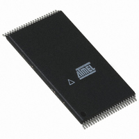
AT49BV320-11TI Atmel, AT49BV320-11TI Datasheet - Page 7

AT49BV320-11TI
Manufacturer Part Number
AT49BV320-11TI
Description
IC FLASH 32MBIT 110NS 48TSOP
Manufacturer
Atmel
Datasheet
1.AT49BV320-11TI.pdf
(30 pages)
Specifications of AT49BV320-11TI
Format - Memory
FLASH
Memory Type
FLASH
Memory Size
32M (4Mx8, 2Mx16)
Speed
110ns
Interface
Parallel
Voltage - Supply
2.65 V ~ 3.3 V
Operating Temperature
-40°C ~ 85°C
Package / Case
48-TSOP
Lead Free Status / RoHS Status
Contains lead / RoHS non-compliant
AT49BV/LV320(T)/321(T)
the system must write the Product ID Exit command to return to the read mode. The
erase/program status bit is a “0” while the erase or program operation is still in progress.
Please see “Status Bit Table” on page 11 for more details.
V
STATUS BIT: The AT49BV/LV32X(T) provides a status bit on I/O3, which provides infor-
PP
mation regarding the voltage level of the VPP pin. During a program or erase operation, if the
voltage on the VPP pin is not high enough to perform the desired operation successfully, the
I/O3 status bit will be a “1”. Once the V
status bit has been set to a “1”, the system must
PP
write the Product ID Exit command to return to the read mode. On the other hand, if the volt-
age level is high enough to perform a program or erase operation successfully, the V
status
PP
bit will output a “0”. Please see “Status Bit Table” on page 11 for more details.
SECTOR LOCKDOWN: Each sector has a programming lockdown feature. This feature pre-
vents programming of data in the designated sectors once the feature has been enabled.
These sectors can contain secure code that is used to bring up the system. Enabling the lock-
down feature will allow the boot code to stay in the device while data in the rest of the device is
updated. This feature does not have to be activated; any sector’s usage as a write-protected
region is optional to the user.
At power-up or reset, all sectors are unlocked. To activate the lockdown for a specific sector,
the six-bus cycle Sector Lockdown command must be issued. Once a sector has been locked
down, the contents of the sector is read-only and cannot be erased or programmed.
SECTOR LOCKDOWN DETECTION: A software method is available to determine if program-
ming of a sector is locked down. When the device is in the software product identification
mode (see “Software Product Identification Entry/Exit” sections on page 25), a read from
address location 00002H within a sector will show if programming the sector is locked down. If
the data on I/O0 is low, the sector can be programmed; if the data on I/O0 is high, the program
lockdown feature has been enabled and the sector cannot be programmed. The software
product identification exit code should be used to return to standard operation.
SECTOR LOCKDOWN OVERRIDE: The only way to unlock a sector that is locked down is
through reset or power-up cycles. After power-up or reset, the content of a sector that is
locked down can be erased and reprogrammed.
ERASE SUSPEND/ERASE RESUME: The Erase Suspend command allows the system to
interrupt a sector or chip erase operation and then program or read data from a different sector
within the memory. After the Erase Suspend command is given, the device requires a maxi-
mum time of 15 µs to suspend the erase operation. After the erase operation has been
suspended, the system can then read data or program data to any other sector within the
device. An address is not required during the Erase Suspend command. During a sector erase
suspend, another sector cannot be erased. To resume the sector erase operation, the system
must write the Erase Resume command. The Erase Resume command is a one-bus cycle
command. The device also supports an erase suspend during a complete chip erase. While
the chip erase is suspended, the user can read from any sector within the memory that is pro-
tected. The command sequence for a chip erase suspend and a sector erase suspend are the
same.
PROGRAM SUSPEND/PROGRAM RESUME: The Program Suspend command allows the
system to interrupt a programming operation and then read data from a different byte/word
within the memory. After the Program Suspend command is given, the device requires a max-
imum of 20 µs to suspend the programming operation. After the programming operation has
been suspended, the system can then read data from any other byte/word within the device.
An address is not required during the program suspend operation. To resume the program-
ming operation, the system must write the Program Resume command. The program suspend
and resume are one-bus cycle commands. The command sequence for the erase suspend
and program suspend are the same, and the command sequence for the erase resume and
program resume are the same.
7
1494H–FLASH–01/03


