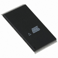
AT49BV320-11TI Atmel, AT49BV320-11TI Datasheet - Page 12

AT49BV320-11TI
Manufacturer Part Number
AT49BV320-11TI
Description
IC FLASH 32MBIT 110NS 48TSOP
Manufacturer
Atmel
Datasheet
1.AT49BV320-11TI.pdf
(30 pages)
Specifications of AT49BV320-11TI
Format - Memory
FLASH
Memory Type
FLASH
Memory Size
32M (4Mx8, 2Mx16)
Speed
110ns
Interface
Parallel
Voltage - Supply
2.65 V ~ 3.3 V
Operating Temperature
-40°C ~ 85°C
Package / Case
48-TSOP
Lead Free Status / RoHS Status
Contains lead / RoHS non-compliant
Command Definition in Hex
Notes:
Absolute Maximum Ratings*
12
Command
Sequence
Read
Chip Erase
Sector Erase
Byte/Word Program
Enter Single Pulse
Program Mode
Single Pulse
Byte/Word Program
Sector Lockdown
Erase/Program
Suspend
Erase/Program
Resume
Product ID Entry
Product ID Exit
Product ID Exit
Program Protection
Register
Lock Protection
Register - Block B
Status of Block B
Protection
Set Configuration
Register
Temperature under Bias ................................ -55°C to +125°C
Storage Temperature ..................................... -65°C to +150°C
All Input Voltages
(including NC Pins)
with Respect to Ground ...................................-0.6V to +6.25V
All Output Voltages
with Respect to Ground .............................-0.6V to V
Voltage on OE and V
with Respect to Ground ...................................-0.6V to +13.0V
1. The DATA FORMAT shown for each bus cycle is as follows; I/O7 - I/O0 (Hex). In word operation I/O15 - I/O8
2. Since A11 is a Don’t Care, AAA can be replaced with 2AA.
3. SA = sector address. Any byte/word address within a sector can be used to designate the sector address (see pages 14 and
4. Once a sector is in the lockdown mode, data in the protected sector cannot be changed unless the chip is reset or power
5. Either one of the Product ID Exit commands can be used.
6. If data bit D1 is “0”, block B is locked. If data bit D1 is “1”, block B can be reprogrammed.
7. The default state (after power-up) of the configuration register is “00”.
AT49BV/LV320(T)/321(T)
are don’t care. The ADDRESS FORMAT shown for each bus cycle is as follows: A11 - A0 (Hex). Address A20 through A11
are don’t care in the word mode. Address A20 through A11 and A-1 are don’t care in the byte mode.
16 for details).
cycled.
(5)
(5)
PP
Cycles
Bus
1
6
6
4
6
1
6
1
1
3
3
1
4
4
4
4
Addr
Addr
Addr
XXX
XXX
XXX
555
555
555
555
555
555
555
555
555
555
555
1st Bus
Cycle
Data
D
AA
AA
AA
AA
D
AA
AA
AA
AA
AA
AA
AA
B0
30
F0
OUT
IN
(1)
AAA
AAA
Addr
AAA
AAA
AAA
AAA
AAA
AAA
AAA
AAA
AAA
2nd Bus
(2)
(2)
Cycle
CC
+ 0.6V
Data
55
55
55
55
55
55
55
55
55
55
55
Addr
555
555
555
555
555
555
555
555
555
555
555
3rd Bus
Cycle
*NOTICE:
Data
A0
F0
C0
C0
D0
80
80
80
80
90
90
Addr
Addr
Addr
XXX
555
555
555
555
080
80
Stresses beyond those listed under “Absolute
Maximum Ratings” may cause permanent dam-
age to the device. This is a stress rating only and
functional operation of the device at these or any
other conditions beyond those indicated in the
operational sections of this specification is not
implied. Exposure to absolute maximum rating
conditions for extended periods may affect
device reliability.
4th Bus
Cycle
00/01
D
Data
OUT
D
D
AA
AA
AA
AA
X0
IN
IN
(6)
(7)
Addr
AAA
AAA
AAA
AAA
5th Bus
Cycle
Data
55
55
55
55
1494H–FLASH–01/03
SA
SA
Addr
555
555
(3)(4)
(3)(4)
6th Bus
Cycle
Data
A0
10
30
60


