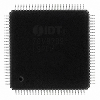
IDT70V9289L9PFI IDT, Integrated Device Technology Inc, IDT70V9289L9PFI Datasheet - Page 8

IDT70V9289L9PFI
Manufacturer Part Number
IDT70V9289L9PFI
Description
IC SRAM 1MBIT 9NS 100TQFP
Manufacturer
IDT, Integrated Device Technology Inc
Datasheet
1.IDT70V9289L9PFI.pdf
(19 pages)
Specifications of IDT70V9289L9PFI
Format - Memory
RAM
Memory Type
SRAM - Dual Port, Synchronous
Memory Size
1M (64K x 16)
Speed
9ns
Interface
Parallel
Voltage - Supply
3 V ~ 3.6 V
Operating Temperature
-40°C ~ 85°C
Package / Case
100-TQFP, 100-VQFP
Density
1Mb
Access Time (max)
20ns
Sync/async
Synchronous
Architecture
SDR
Clock Freq (max)
40MHz
Operating Supply Voltage (typ)
3.3V
Address Bus
32b
Package Type
TQFP
Operating Temp Range
-40C to 85C
Number Of Ports
2
Supply Current
240mA
Operating Supply Voltage (min)
3V
Operating Supply Voltage (max)
3.6V
Operating Temperature Classification
Industrial
Mounting
Surface Mount
Pin Count
100
Word Size
16b
Number Of Words
64K
Lead Free Status / RoHS Status
Contains lead / RoHS non-compliant
Other names
70V9289L9PFI
800-1401
800-1401
Available stocks
Company
Part Number
Manufacturer
Quantity
Price
Company:
Part Number:
IDT70V9289L9PFI
Manufacturer:
IDT, Integrated Device Technology Inc
Quantity:
10 000
DC Electrical Characteristics Over the Operating
Temperature and Supply Voltage Range
DC Electrical Characteristics Over the Operating
Temperature Supply Voltage Range
NOTE:
1. At V
NOTES:
1. At f = f
2. f = 0 means no address, clock, or control lines change. Applies only to input at CMOS level standby.
3. Port "A" may be either left or right port. Port "B" is the opposite from port "A".
4. V
5. CE
6. This speed grade available in PK-128 package only.
IDT70V9389/289L
High-Speed 3.3V 64K x18/x16 Dual-Port Synchronous Pipelined Static RAM
Symbol
Symbol
levels of GND to 3V.
CE
CE
CE
"X" represents "L" for left port or "R" for right port.
V
V
|I
|I
I
I
I
I
I
SB2
SB3
SB4
LO
SB1
DD
OL
OH
DD
LI
X
X
X
X
|
|
DD
= 3.3V, T
< 0.2V means CE
> V
= V
= V
MAX
< 2.0V input leakages are undefined.
DD
IH
IL
Input Leakage Current
Output Leakage Current
Output Low Voltage
Output High Voltage
Dynamic Operating
Current (Both
Ports Active)
Standby Current
(Both Ports - TTL
Level Inputs)
Standby
Current (One
Port - TTL
Level Inputs)
Full Standby
Current (Both
Ports - CMOS
Level Inputs)
Full Standby
Current (One
Port - CMOS
Level Inputs)
, address and control lines (except Output Enable) are cycling at the maximum frequency clock cycle of 1/t
means CE
means CE
- 0.2V means CE
A
Parameter
= 25°C for Typ, and are not production tested. I
Parameter
0X
0X
0X
= V
= V
< 0.2V and CE
IL
IH
0X
and CE
Outputs Disabled,
Both Ports CE
Outputs Disabled, f = f
CE
f = f
CE
f = f
CE
CE
Active Port Outputs Disabled,
f=f
CE
V
V
CE
CE
V
V
or CE
> V
IN
IN
IN
IN
MAX
L
L
"A"
"B"
R
"A"
"B"
(1)
MAX
MAX
> V
< 0.2V, f = 0
> V
< 0.2V, Active Port,
and CE
= CE
> V
CC
= V
(1)
= V
< 0.2V and
> V
1X
Test Condition
DD
DD
(1)
(1)
1X
DD
- 0.2V or CE
R
IH
IL
DD
= V
- 0.2V or
- 0.2V or
(5)
= V
= V
- 0.2V,
1X
R
and
= V
- 0.2V
L
IL
> V
IH
and
IH
(2)
IL
V
CE = V
I
I
,
OL
OH
(5)
DD
DD
= +4mA
MAX
= -4mA
- 0.2V
= 3.6V, V
1X
(1)
< 0.2V
IH
or CE
COM'L
IND
COM'L
IND
COM'L
IND
COM'L
IND
COM'L
IND
Version
IN
1
= 0V to V
= V
DD DC
IL
L
L
L
L
L
L
L
L
L
L
, V
(f=0) = 90mA (Typ).
OUT
Typ.
DD
70V9389/289L6
220
145
145
____
____
____
0.4
____
____
60
6.42
Com'l Only
= 0V to V
(4)
(3)
Test Conditions
8
(V
Max.
280
185
180
____
____
____
____
____
85
2
DD
(6)
DD
(V
DD
= 3.3V ± 0.3V)
Typ.
200
130
130
____
____
____
0.4
____
____
70V9389/289L7
50
= 3.3V ± 0.3V)
Com'l Only
(4)
Industrial & Commercial Temperature Ranges
Max.
250
165
160
____
____
____
____
____
75
2
Typ.
175
180
110
110
0.4
0.4
100
100
40
50
70V9389/289L9
CYC
Com'l & Ind
(4)
, using "AC TEST CONDITIONS" at input
Max.
240
230
145
155
140
155
65
70
2
2
Min.
2.4
70V9389/289L
___
___
___
Typ.
70V9389/289L12
150
____
____
____
0.4
____
____
30
95
90
Com'l Only
(4)
Max.
0.4
___
5
5
Max.
200
130
125
____
____
____
____
____
50
2
4856 tbl 08
4856 tbl 09
Unit
µ A
µ A
V
V
Unit
mA
mA
mA
mA
mA


