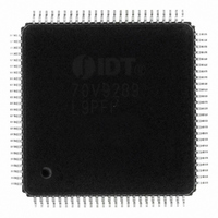
IDT70V9289L9PFI IDT, Integrated Device Technology Inc, IDT70V9289L9PFI Datasheet - Page 7

IDT70V9289L9PFI
Manufacturer Part Number
IDT70V9289L9PFI
Description
IC SRAM 1MBIT 9NS 100TQFP
Manufacturer
IDT, Integrated Device Technology Inc
Datasheet
1.IDT70V9289L9PFI.pdf
(19 pages)
Specifications of IDT70V9289L9PFI
Format - Memory
RAM
Memory Type
SRAM - Dual Port, Synchronous
Memory Size
1M (64K x 16)
Speed
9ns
Interface
Parallel
Voltage - Supply
3 V ~ 3.6 V
Operating Temperature
-40°C ~ 85°C
Package / Case
100-TQFP, 100-VQFP
Density
1Mb
Access Time (max)
20ns
Sync/async
Synchronous
Architecture
SDR
Clock Freq (max)
40MHz
Operating Supply Voltage (typ)
3.3V
Address Bus
32b
Package Type
TQFP
Operating Temp Range
-40C to 85C
Number Of Ports
2
Supply Current
240mA
Operating Supply Voltage (min)
3V
Operating Supply Voltage (max)
3.6V
Operating Temperature Classification
Industrial
Mounting
Surface Mount
Pin Count
100
Word Size
16b
Number Of Words
64K
Lead Free Status / RoHS Status
Contains lead / RoHS non-compliant
Other names
70V9289L9PFI
800-1401
800-1401
Available stocks
Company
Part Number
Manufacturer
Quantity
Price
Company:
Part Number:
IDT70V9289L9PFI
Manufacturer:
IDT, Integrated Device Technology Inc
Quantity:
10 000
Truth Table II—Address Counter Control
Recommended Operating
Temperature and Supply Voltage
Absolute Maximum Ratings
NOTES:
1. This is the parameter T
NOTES:
1. Stresses greater than those listed under ABSOLUTE MAXIMUM RATINGS may
2. V
3. Ambient Temperature Under DC Bias. No AC Conditions. Chip Deselected.
NOTES:
1. "H" = V
2. CE
3. Outputs configured in Flow-Through Output mode; if outputs are in Pipelined mode the data out will be delayed by one cycle.
4. ADS and CNTRST are independent of all other signals including CE
5. The address counter advances if CNTEN = V
Commercial
Industrial
I
V
T
T
T
OUT
Address
BIAS
STG
JN
External
IDT70V9389/289L
High-Speed 3.3V 64K x18/x16 Dual-Port Synchronous Pipelined Static RAM
TERM
Symbol
cause permanent damage to the device. This is a stress rating only and functional
operation of the device at these or any other conditions above those indicated
in the operational sections of this specification is not implied. Exposure to absolute
maximum rating conditions for extended periods may affect reliability.
maximum, and is limited to < 20mA for the period of V
An
An
TERM
X
X
(3)
0
(2)
, LB, UB, and OE = V
Grade
must not exceed V
IH,
"L" = V
Previous
Address
Internal
GND
Under Bias
Storage
Junction Temperature
DC Output Current
Terminal Voltage
with Respect to
Temperature
Temperature
Ap
Ap
X
X
IL,
"X" = Don't Care.
Rating
Address
A
Internal
Ap + 1
-40
Temperature
. This is the "instant on" case temperature.
DD
Used
0
IL
Ap
An
O
0
; CE
C to +70
O
Ambient
+0.3V for more than 25% of the cycle time or 10ns
C to +85
1
and R/W = V
CLK
O
↑
↑
↑
↑
O
C
(2)
C
IL
ADS
Commercial
& Industrial
-0.5 to +4.6
-55 to +125
-65 to +150
IH
GND
on the rising edge of CLK, regardless of all other signals including CE
X
L
H
H
0V
0V
.
(4)
+150
50
TERM
CNTEN
(1)
3.3V
3.3V
X
X
H
L
> V
(5)
DD
V
+
+
DD
+ 0.3V.
0.3V
0.3V
0
CNTRST
4856 tbl 04
, CE
4856 tbl 06
Unit
mA
(1)
o
o
o
V
C
C
C
L
H
H
H
(4)
1
, UB and LB.
6.42
7
Recommended DC Operating
Conditions
NOTES:
1. V
2. V
Capacitance
(T
NOTES:
1. These parameters are determined by device characterization, but are not
2. 3dV references the interpolated capacitance when the input and output switch
3. C
D
Symbol
Symbol
D
D
D
I/O
I/O
A
C
production tested.
from 0V to 3V or from 3V to 0V.
V
V
I/O
I/O
I/O
V
V
C
(p+1)
IL
TERM
OUT
OUT
DD
SS
IH
IL
(1,2)
(p)
= +25°C, f = 1.0MH
(3)
(0)
(n)
IN
> -1.5V for pulse width less than 10 ns.
(3)
also references C
must not exceed V
Supply Voltage
Ground
Input High Voltage
Input Low Voltage
Input Capacitance
Output Capacitance
Counter Reset to Address 0
External Address Loaded into Counter
External Address Blocked—Counter disabled (Ap reused)
Counter Enabled—Internal Address generation
Parameter
Industrial & Commercial Temperature Ranges
Parameter
I/O
(1)
.
DD
+0.3V.
0
, CE
Z
-0.3
Min.
)
3.0
2.0
0
1
(1)
, UB and LB.
MODE
Conditions
V
V
OUT
Typ.
3.3
____
____
IN
0
= 3dV
= 3dV
V
(2)
DD
Max.
+0.3V
3.6
0.8
0
Max.
10
9
(2)
4856 tbl 03
4856 tbl 05
4856 tbl 07
Unit
Unit
pF
pF
V
V
V
V


