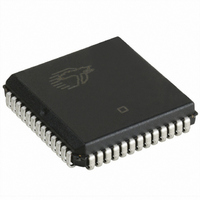
CY7C131-55JXC Cypress Semiconductor Corp, CY7C131-55JXC Datasheet - Page 8

CY7C131-55JXC
Manufacturer Part Number
CY7C131-55JXC
Description
IC SRAM 8KBIT 55NS 52PLCC
Manufacturer
Cypress Semiconductor Corp
Type
Asynchronousr
Datasheet
1.CY7C131-55JXC.pdf
(19 pages)
Specifications of CY7C131-55JXC
Memory Size
8K (1K x 8)
Package / Case
52-PLCC
Format - Memory
RAM
Memory Type
SRAM - Dual Port, Asynchronous
Speed
55ns
Interface
Parallel
Voltage - Supply
4.5 V ~ 5.5 V
Operating Temperature
0°C ~ 70°C
Access Time
55 ns
Supply Voltage (max)
5.5 V
Supply Voltage (min)
4.5 V
Maximum Operating Current
110 mA
Organization
1 K x 8
Maximum Operating Temperature
+ 70 C
Minimum Operating Temperature
- 40 C
Mounting Style
SMD/SMT
Number Of Ports
2
Operating Supply Voltage
5 V
Density
8Kb
Access Time (max)
55ns
Sync/async
Asynchronous
Architecture
Not Required
Clock Freq (max)
Not RequiredMHz
Operating Supply Voltage (typ)
5V
Address Bus
20b
Package Type
PLCC
Operating Temp Range
0C to 70C
Supply Current
110mA
Operating Supply Voltage (min)
4.5V
Operating Supply Voltage (max)
5.5V
Operating Temperature Classification
Commercial
Mounting
Surface Mount
Pin Count
52
Word Size
8b
Number Of Words
1K
Lead Free Status / RoHS Status
Lead free / RoHS Compliant
Lead Free Status / RoHS Status
Lead free / RoHS Compliant, Lead free / RoHS Compliant
Other names
428-1791
CY7C131-55JXC
CY7C131-55JXC
Available stocks
Company
Part Number
Manufacturer
Quantity
Price
Company:
Part Number:
CY7C131-55JXC
Manufacturer:
LATTICE
Quantity:
539
Company:
Part Number:
CY7C131-55JXC
Manufacturer:
Cypress Semiconductor Corp
Quantity:
10 000
Company:
Part Number:
CY7C131-55JXCT
Manufacturer:
CYPRESS
Quantity:
924
Company:
Part Number:
CY7C131-55JXCT
Manufacturer:
Cypress Semiconductor Corp
Quantity:
10 000
Switching Characteristics
Document #: 38-06002 Rev. *E
t
t
t
t
t
t
t
t
t
t
t
t
t
t
t
t
t
t
t
t
t
t
t
t
t
t
t
t
t
t
t
t
t
t
t
t
t
RC
AA
OHA
ACE
DOE
LZOE
HZOE
LZCE
HZCE
PU
PD
WC
SCE
AW
HA
SA
PWE
SD
HD
HZWE
LZWE
BLA
BHA
BLC
BHC
PS
WB
WH
BDD
DDD
WDD
WINS
EINS
INS
OINR
EINR
INR
Read Cycle
Write Cycle
Busy/Interrupt Timing
Interrupt Timing
Parameter
[18]
[16]
Read Cycle Time
Address to Data Valid
Data Hold from Address Change
CE LOW to Data Valid
OE LOW to Data Valid
OE LOW to Low Z
OE HIGH to High Z
CE LOW to Low Z
CE HIGH to High Z
CE LOW to Power Up
CE HIGH to Power Down
Write Cycle Time
CE LOW to Write End
Address Setup to Write End
Address Hold from Write End
Address Setup to Write Start
R/W Pulse Width
Data Setup to Write End
Data Hold from Write End
R/W LOW to High Z
R/W HIGH to Low Z
BUSY LOW from Address Match
BUSY HIGH from Address Mismatch
BUSY LOW from CE LOW
BUSY HIGH from CE HIGH
Port Set Up for Priority
R/W LOW after BUSY LOW
R/W HIGH after BUSY HIGH
BUSY HIGH to Valid Data
Write Data Valid to Read Data Valid
Write Pulse to Data Delay
R/W to INTERRUPT Set Time
CE to INTERRUPT Set Time
Address to INTERRUPT Set Time
OE to INTERRUPT Reset Time
CE to INTERRUPT Reset Time
Address to INTERRUPT Reset Time
Description
[10, 14, 15]
[10, 14, 15]
[15]
[15]
[10, 14, 15]
[10, 14, 15]
Over the Operating Range
[13]
[10]
[13]
[13]
[10]
[17]
[17]
[17]
[17]
[17]
[7,12]
Min
35
35
30
30
25
15
30
0
3
5
0
2
0
0
0
5
0
7C130-35
7C131-35
7C140-35
7C141-35
Note 19
Note 19
Max
35
35
20
20
20
35
20
20
20
20
35
25
25
25
25
25
25
20
Min
45
45
35
35
30
20
35
7C130-45
7C131-45
7C140-45
7C141-45
0
3
5
0
2
0
0
0
5
0
Note 19
Note 19
Max
CY7C130, CY7C130A
CY7C131, CY7C131A
45
45
25
20
20
35
20
25
25
25
25
45
35
35
35
35
35
35
CY7C140, CY7C141
Min
55
55
40
40
30
20
35
7C130-55
7C131-55
7C140-55
7C141-55
0
3
5
0
2
0
0
0
5
0
Note 19
Note 19
Max
30
45
45
55
55
25
25
25
35
25
30
30
30
45
45
45
45
45
Page 8 of 19
Unit
ns
ns
ns
ns
ns
ns
ns
ns
ns
ns
ns
ns
ns
ns
ns
ns
ns
ns
ns
ns
ns
ns
ns
ns
ns
ns
ns
ns
ns
ns
ns
ns
ns
ns
ns
ns
ns
[+] Feedback


