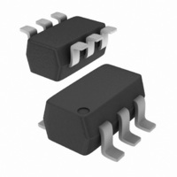
74AVCH1T45GW,125 NXP Semiconductors, 74AVCH1T45GW,125 Datasheet - Page 3

74AVCH1T45GW,125
Manufacturer Part Number
74AVCH1T45GW,125
Description
IC TRANSCVR TRI-ST DL SPLY SC88
Manufacturer
NXP Semiconductors
Series
74AVCHr
Datasheet
1.74AVCH1T45GW125.pdf
(22 pages)
Specifications of 74AVCH1T45GW,125
Output Type
Logic
Package / Case
SC-70-6, SC-88, SOT-363
Logic Function
Translator, Bidirectional, 3-State
Number Of Bits
2
Input Type
Logic
Number Of Channels
2
Number Of Outputs/channel
1
Differential - Input:output
No/No
Propagation Delay (max)
2.7ns
Voltage - Supply
0.8 V ~ 3.6 V
Operating Temperature
-40°C ~ 125°C
Supply Voltage
0.8 V ~ 3.6 V
Logic Family
AVC
Number Of Channels Per Chip
1
Input Level
CMOS
Output Level
CMOS
High Level Output Current
- 12 mA
Low Level Output Current
12 mA
Supply Voltage (max)
3.6 V
Supply Voltage (min)
0.8 V
Maximum Operating Temperature
+ 125 C
Function
Bus Transceiver with Voltage Translation
Input Bias Current (max)
24 uA
Minimum Operating Temperature
- 40 C
Mounting Style
SMD/SMT
Polarity
Non-Inverting
Logic Type
CMOS
Number Of Circuits
1
Data Rate
-
Lead Free Status / RoHS Status
Lead free / RoHS Compliant
Data Rate
-
Lead Free Status / Rohs Status
Lead free / RoHS Compliant
Other names
74AVCH1T45GW-G
74AVCH1T45GW-G
935284156125
74AVCH1T45GW-G
935284156125
NXP Semiconductors
6. Pinning information
Table 3.
7. Functional description
Table 4.
[1]
[2]
[3]
[4]
74AVCH1T45_2
Product data sheet
Symbol
V
GND
A
B
DIR
V
Supply voltage
V
0.8 V to 3.6 V
0.8 V to 3.6 V
GND
Fig 3.
CC(A)
CC(B)
CC(A)
H = HIGH voltage level; L = LOW voltage level; X = don’t care; Z = high-impedance OFF-state.
The input circuit of the data I/O is always active.
The DIR input circuit is referenced to V
If at least one of V
[4]
, V
CC(B)
Pin configuration SOT363
Pin description
Function table
V
CC(A)
GND
6.1 Pinning
6.2 Pin description
A
CC(A)
Pin
1
2
3
4
5
6
1
2
3
74AVCH1T45
or V
[1]
CC(B)
001aag887
Input
DIR
L
H
X
is at GND level, the device goes into Suspend mode.
[3]
6
5
4
CC(A)
V
DIR
B
CC(B)
.
Rev. 02 — 5 May 2009
Description
supply voltage port A and DIR
ground (0 V)
data input or output
data input or output
direction control
supply voltage port B
Input/output
A
A = B
input
Z
Fig 4.
Pin configuration SOT886
Dual supply translating transceiver; 3-state
[2]
V
CC(A)
GND
A
Transparent top view
74AVCH1T45
1
2
3
74AVCH1T45
B
input
B = A
Z
001aag888
6
5
4
V
DIR
B
CC(B)
© NXP B.V. 2009. All rights reserved.
3 of 22


