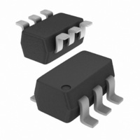
74AVCH1T45GW,125 NXP Semiconductors, 74AVCH1T45GW,125 Datasheet - Page 11

74AVCH1T45GW,125
Manufacturer Part Number
74AVCH1T45GW,125
Description
IC TRANSCVR TRI-ST DL SPLY SC88
Manufacturer
NXP Semiconductors
Series
74AVCHr
Datasheet
1.74AVCH1T45GW125.pdf
(22 pages)
Specifications of 74AVCH1T45GW,125
Output Type
Logic
Package / Case
SC-70-6, SC-88, SOT-363
Logic Function
Translator, Bidirectional, 3-State
Number Of Bits
2
Input Type
Logic
Number Of Channels
2
Number Of Outputs/channel
1
Differential - Input:output
No/No
Propagation Delay (max)
2.7ns
Voltage - Supply
0.8 V ~ 3.6 V
Operating Temperature
-40°C ~ 125°C
Supply Voltage
0.8 V ~ 3.6 V
Logic Family
AVC
Number Of Channels Per Chip
1
Input Level
CMOS
Output Level
CMOS
High Level Output Current
- 12 mA
Low Level Output Current
12 mA
Supply Voltage (max)
3.6 V
Supply Voltage (min)
0.8 V
Maximum Operating Temperature
+ 125 C
Function
Bus Transceiver with Voltage Translation
Input Bias Current (max)
24 uA
Minimum Operating Temperature
- 40 C
Mounting Style
SMD/SMT
Polarity
Non-Inverting
Logic Type
CMOS
Number Of Circuits
1
Data Rate
-
Lead Free Status / RoHS Status
Lead free / RoHS Compliant
Data Rate
-
Lead Free Status / Rohs Status
Lead free / RoHS Compliant
Other names
74AVCH1T45GW-G
74AVCH1T45GW-G
935284156125
74AVCH1T45GW-G
935284156125
NXP Semiconductors
Table 11.
Voltages are referenced to GND (ground = 0 V); for test circuit see
[1]
74AVCH1T45_2
Product data sheet
Symbol Parameter
V
t
t
t
V
t
t
t
V
t
t
t
V
t
t
t
V
t
t
t
pd
dis
en
pd
dis
en
pd
dis
en
pd
dis
en
pd
dis
en
CC(A)
CC(A)
CC(A)
CC(A)
CC(A)
t
t
pd
en
is the same as t
is a calculated value using the formula shown in
= 1.1 V to 1.3 V
= 1.4 V to 1.6 V
= 1.65 V to 1.95 V
= 2.3 V to 2.7 V
= 3.0 V to 3.6 V
propagation
delay
disable time
enable time
propagation
delay
disable time
enable time
propagation
delay
disable time
enable time
propagation
delay
disable time
enable time
propagation
delay
disable time
enable time
Dynamic characteristics for temperature range 40 C to +85 C
PLH
and t
Conditions
A to B
B to A
DIR to A
DIR to B
DIR to A
DIR to B
A to B
B to A
DIR to A
DIR to B
DIR to A
DIR to B
A to B
B to A
DIR to A
DIR to B
DIR to A
DIR to B
A to B
B to A
DIR to A
DIR to B
DIR to A
DIR to B
A to B
B to A
DIR to A
DIR to B
DIR to A
DIR to B
PHL
; t
dis
is the same as t
V
1.2 V
Min
CC(B)
1.0
1.0
2.2
2.2
1.0
1.0
1.6
2.0
1.0
1.0
1.6
1.8
1.0
1.0
1.5
1.7
1.0
1.0
1.5
1.7
-
-
-
-
-
-
-
-
-
-
0.1 V
Max
17.4
17.8
14.4
14.3
13.9
13.2
13.0
11.4
13.3
11.8
9.0
9.0
8.8
8.4
8.0
6.8
6.3
7.6
7.7
6.1
5.5
7.8
7.2
5.7
4.2
7.3
7.1
6.1
4.7
7.2
Section 13.4 “Enable times”
PLZ
Rev. 02 — 5 May 2009
and t
1.5 V
Min
0.7
0.8
2.2
1.8
0.7
0.8
1.6
1.8
0.6
0.7
1.6
1.8
0.5
0.6
1.5
2.0
0.5
0.6
1.5
0.7
-
-
-
-
-
-
-
-
-
-
PHZ
; t
en
0.1 V 1.8 V
Max
14.7
15.6
11.3
11.7
10.3
10.6
6.8
8.0
8.8
6.7
5.4
5.4
6.3
5.9
5.1
4.6
5.5
5.7
4.7
3.8
4.2
5.2
9.0
8.9
4.5
3.6
4.7
5.5
9.1
9.2
is the same as t
Figure
Min
Dual supply translating transceiver; 3-state
0.6
0.7
2.2
2.0
0.6
0.7
1.6
1.6
0.5
0.5
1.6
1.4
0.5
0.5
1.5
1.5
0.5
0.5
1.5
0.6
7; for wave forms see
-
-
-
-
-
-
-
-
-
-
0.15 V 2.5 V
PZL
Max
14.6
14.9
11.1
10.9
10.2
[1]
6.1
7.7
8.8
6.9
4.6
5.1
6.3
6.0
4.3
4.4
5.5
5.8
9.8
3.9
3.4
4.2
5.1
8.5
8.1
3.7
3.1
4.7
5.5
8.6
8.4
and t
PZH
Min
0.5
0.6
2.2
1.7
0.5
0.6
1.6
1.2
0.5
0.5
1.6
1.0
0.5
0.5
1.5
0.6
0.5
0.5
1.5
0.7
-
-
-
-
-
-
-
-
-
-
.
74AVCH1T45
0.2 V
Figure 5
Max
13.4
14.5
10.0
5.7
7.2
8.8
6.2
3.7
4.7
6.3
4.8
9.5
3.4
3.9
5.5
4.5
8.4
8.9
3.0
3.0
4.2
4.2
7.2
7.2
2.8
2.6
4.7
4.1
6.7
7.5
3.3 V
© NXP B.V. 2009. All rights reserved.
Min
0.5
0.5
2.2
2.4
0.5
0.5
1.6
1.7
0.5
0.5
1.6
1.5
0.5
0.5
1.5
1.1
0.5
0.5
1.5
1.7
and
-
-
-
-
-
-
-
-
-
-
Figure
0.3 V
Max
14.3
14.9
10.0
6.1
7.1
8.8
7.2
3.5
4.5
6.3
5.5
9.8
3.1
3.7
5.5
5.2
8.9
8.6
2.6
2.8
4.2
4.8
7.6
6.8
2.4
2.4
4.7
4.7
7.1
7.1
6.
11 of 22
Unit
ns
ns
ns
ns
ns
ns
ns
ns
ns
ns
ns
ns
ns
ns
ns
ns
ns
ns
ns
ns
ns
ns
ns
ns
ns
ns
ns
ns
ns
ns


