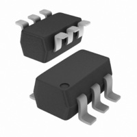
74AVCH1T45GW,125 NXP Semiconductors, 74AVCH1T45GW,125 Datasheet - Page 17

74AVCH1T45GW,125
Manufacturer Part Number
74AVCH1T45GW,125
Description
IC TRANSCVR TRI-ST DL SPLY SC88
Manufacturer
NXP Semiconductors
Series
74AVCHr
Datasheet
1.74AVCH1T45GW125.pdf
(22 pages)
Specifications of 74AVCH1T45GW,125
Output Type
Logic
Package / Case
SC-70-6, SC-88, SOT-363
Logic Function
Translator, Bidirectional, 3-State
Number Of Bits
2
Input Type
Logic
Number Of Channels
2
Number Of Outputs/channel
1
Differential - Input:output
No/No
Propagation Delay (max)
2.7ns
Voltage - Supply
0.8 V ~ 3.6 V
Operating Temperature
-40°C ~ 125°C
Supply Voltage
0.8 V ~ 3.6 V
Logic Family
AVC
Number Of Channels Per Chip
1
Input Level
CMOS
Output Level
CMOS
High Level Output Current
- 12 mA
Low Level Output Current
12 mA
Supply Voltage (max)
3.6 V
Supply Voltage (min)
0.8 V
Maximum Operating Temperature
+ 125 C
Function
Bus Transceiver with Voltage Translation
Input Bias Current (max)
24 uA
Minimum Operating Temperature
- 40 C
Mounting Style
SMD/SMT
Polarity
Non-Inverting
Logic Type
CMOS
Number Of Circuits
1
Data Rate
-
Lead Free Status / RoHS Status
Lead free / RoHS Compliant
Data Rate
-
Lead Free Status / Rohs Status
Lead free / RoHS Compliant
Other names
74AVCH1T45GW-G
74AVCH1T45GW-G
935284156125
74AVCH1T45GW-G
935284156125
NXP Semiconductors
74AVCH1T45_2
Product data sheet
13.3 Power-up considerations
13.4 Enable times
The device is designed such that no special power-up sequence is required other than
GND being applied first.
Table 17.
The enable times for the 74AVCH1T45 are calculate from the following formulas:
In a bidirectional application, these enable times provide the maximum delay from the time
the DIR bit is switched until an output is expected. For example, if the 74AVCH1T45
initially is transmitting from A to B, then the DIR bit is switched, the B port of the device
must be disabled before presenting it with an input. After the B port has been disabled, an
input signal applied to it appears on the corresponding A port after the specified
propagation delay.
V
0 V
0.8 V
1.2 V
1.5 V
1.8 V
2.5 V
3.3 V
•
•
CC(A)
t
t
en
en
(DIR to A) = t
(DIR to B) = t
V
0 V
0
0.1
0.1
0.1
0.1
0.1
0.1
Typical total supply current (I
CC(B)
0.8 V
0.1
0.1
0.1
0.1
0.1
0.7
2.3
dis
dis
(DIR to B) + t
(DIR to A) + t
Rev. 02 — 5 May 2009
1.2 V
0.1
0.1
0.1
0.1
0.1
0.3
1.4
pd
pd
CC(A)
(B to A)
(A to B)
1.5 V
0.1
0.1
0.1
0.1
0.1
0.1
0.9
Dual supply translating transceiver; 3-state
+ I
CC(B)
1.8 V
0.1
0.1
0.1
0.1
0.1
0.1
0.5
)
2.5 V
0.1
0.7
0.3
0.1
0.1
0.1
0.1
74AVCH1T45
3.3 V
0.1
2.3
1.4
0.9
0.5
0.1
0.1
© NXP B.V. 2009. All rights reserved.
Unit
A
A
A
A
A
A
A
17 of 22


