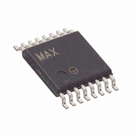
MAX13003EEUE+ Maxim Integrated Products, MAX13003EEUE+ Datasheet - Page 9

MAX13003EEUE+
Manufacturer Part Number
MAX13003EEUE+
Description
IC LEVEL TRANS 6CH 16-TSSOP
Manufacturer
Maxim Integrated Products
Datasheet
1.MAX13003EEUE.pdf
(25 pages)
Specifications of MAX13003EEUE+
Logic Function
Translator, Bidirectional
Number Of Bits
6
Input Type
CMOS
Output Type
CMOS
Data Rate
20Mbps
Number Of Channels
1
Number Of Outputs/channel
6
Differential - Input:output
No/No
Propagation Delay (max)
15ns
Voltage - Supply
1.5 V ~ 3.6 V
Operating Temperature
-40°C ~ 85°C
Package / Case
16-TSSOP
Supply Voltage
1.5 V ~ 3.6 V
Lead Free Status / RoHS Status
Lead free / RoHS Compliant
(V
MAX13000E/MAX13003E
CC
TSSOP
= +3.3V, V
10
11
12
13
14
15
16
1
2
3
4
5
6
7
8
9
PIN
L
= +0.9V, T
0.25
0.20
0.15
0.10
0.05
0
UCSP
_______________________________________________________________________________________
C4
C3
D4
D3
D2
D1
C2
C1
B1
B2
A1
A2
A3
A4
B3
B4
0
5
A
10
= +25°C, MAX13003E.)
I
15
OLC
Ultra-Low-Voltage Level Translators
20
V
FOR V
I
OLC
OLC
I/OV
I/OV
I/OV
I/OV
I/OV
I/OV
V
NAME
I/OV
I/OV
I/OV
I/OV
I/OV
I/OV
25 30 35 40 45 50
CC
GND
V
(µA)
EN
vs.
V
CC
CC
= +2.5V
L
CC
CC
CC
CC
CC
CC
V
L
L
L
L
L
L
CC
SIDE
1
2
3
4
5
6
6
5
4
3
2
1
= +1.8V
V
Typical Operating Characteristics (continued)
CC
= +3.3V
CMOS Input/Output 1, Referenced to V
CMOS Input/Output 2, Referenced to V
CMOS Input/Output 3, Referenced to V
Logic Input Voltage, +0.9V ≤ V
capacitor.
Enable Input. When EN is pulled low, I/O V
V
CMOS Input/Output 4, Referenced to V
CMOS Input/Output 5, Referenced to V
CMOS Input/Output 6, Referenced to V
CMOS Input/Output 6, Referenced to V
CMOS Input/Output 5, Referenced to V
CMOS Input/Output 4, Referenced to V
Ground
V
capacitor. For full ESD protection, use a 1µF bypass capacitor on V
CMOS Input/Output 3, Referenced to V
CMOS Input/Output 2, Referenced to V
CMOS Input/Output 1, Referenced to V
L
CC
6 are tri-stated. Drive EN high (V
Input Voltage, +1.5V ≤ V
3.5
3.0
2.5
2.0
1.5
1.0
0
CC
5
L
≤ V
≤ 3.6V. Bypass V
10
L
FUNCTION
CC
I
) for normal operation.
OHC
15
. Bypass V
L
L
L
L
L
L
CC
CC
CC
CC
CC
CC
20
V
V
V
FOR V
V
I
CC
CC
OHC
CC
OHC
CC
= +3.3V
= +1.8V
25 30 35 40 45 50
= +2.5V
(µA)
vs.
CC
1 to I/O V
SIDE
L
CC
Pin Descriptions
to GND with a 0.1µF
to GND with a 0.1µF
CC
6 and I/O V
CC
L
1 to I/O
.
9


