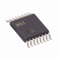
MAX13003EEUE+ Maxim Integrated Products, MAX13003EEUE+ Datasheet - Page 14

MAX13003EEUE+
Manufacturer Part Number
MAX13003EEUE+
Description
IC LEVEL TRANS 6CH 16-TSSOP
Manufacturer
Maxim Integrated Products
Datasheet
1.MAX13003EEUE.pdf
(25 pages)
Specifications of MAX13003EEUE+
Logic Function
Translator, Bidirectional
Number Of Bits
6
Input Type
CMOS
Output Type
CMOS
Data Rate
20Mbps
Number Of Channels
1
Number Of Outputs/channel
6
Differential - Input:output
No/No
Propagation Delay (max)
15ns
Voltage - Supply
1.5 V ~ 3.6 V
Operating Temperature
-40°C ~ 85°C
Package / Case
16-TSSOP
Supply Voltage
1.5 V ~ 3.6 V
Lead Free Status / RoHS Status
Lead free / RoHS Compliant
The MAX13000E–MAX13005E logic-level translators
provide the level shifting necessary to allow data trans-
fer in multivoltage systems. Externally applied voltages,
V
device. Logic signals present on the V
device appear as higher voltage logic signals on the
V
The MAX13000E/MAX13003E are bidirectional level
translators allowing data translation in either direction
(V
DIRECTION input. The MAX13001E/MAX13002E/
MAX13004E/MAX13005E unidirectional level translators
level shift data in one direction (V
V
MAX13002E/MAX13004E/MAX13005E unidirectional
translators’ inputs have the capability to interface with
both CMOS and open-drain (OD) outputs. For more
information, see the Ordering Information section and
the Input Driver Requirements section.
The MAX13000E–MAX13005E accept V
+3.6V. All devices have V
+3.6V, making them ideal for data transfer between
low-voltage ASICs/PLDs and higher voltage systems.
The MAX13000E–MAX13005E feature low V
cent supply current of less than 4µA, and V
supply current of less than 2µA when in shutdown. The
MAX13000E–MAX13005E have ±15kV ESD protection
on the V
that route signals externally. The ESD protection is
specified using the Human Body Model (HBM).The
MAX13000E/MAX13001E/MAX13002E operate at a
guaranteed 230kbps data rate. The MAX13003E/
MAX13004E/MAX13005E operate at a guaranteed
20Mbps data rate when V
For normal operation, ensure that +1.5V ≤ V
and +0.9V ≤ V
V
within the absolute maximum ratings (see the Absolute
Maximum Ratings section). During power-supply
sequencing, when V
up, 1mA of current can be sourced to each load on the
V
The MAX13000E–MAX13005E are designed to have
V
part will not be damaged and will not latch up. To pre-
vent excessive leakage currents in either the I/O or
supply lines, the I/O on the V
high state.
Ultra-Low-Voltage Level Translators
14
CC
CC
L
L
CC
L
L
) on any single data line. The MAX13001E/
side, yet the device does not latch up.
≥ V
↔ V
side of the device, and vice-versa.
______________________________________________________________________________________
≥ V
and V
CC
CC
L
CC
does not damage the device whenever V
at all times; however, if V
) on any single data line without the use of a
L
, set the logic levels on each side of the
side for greater protection in applications
L
≤ V
CC
CC
Detailed Description
. During power-up sequencing,
is floating and V
CC
CC
> +1.65V.
L
ranging from +1.5V to
side must be left in the
Level Translation
L
CC
→ V
is turned off, the
L
CC
from +0.9V to
L
L
CC
side of the
L
is powered
or V
CC
quiescent
≤ +3.6V,
quies-
CC
L
→
is
The maximum data rate for the MAX13000E–
MAX13005E depends heavily on the load capacitance
(see the Typical Operating Characteristics), output
impedance of the driver, and the operational voltage
range (see the Timing Characteristics table).
The MAX13001E/MAX13002E/MAX13004E/MAX13005E
have input stages specifically designed to accommo-
date external open-drain drivers. When using open-
drain
MAX13004E/MAX13005E operate in a unidirectional-
only mode, translating from the OD side to the CMOS
side. For improved performance, the rise- and fall-time
accelerators are present on both the CMOS and the
OD side. See the Input-Driver Requirement section. Do
not use pullup resistors greater than 15kΩ for proper
operation, and smaller pullup resistance may be need-
ed for higher speed operation.
The MAX13000E–MAX13005E feature four different
architectures based on the speed of the part, as well as
on whether the translator is a CMOS-to-CMOS transla-
tor, or whether it is an OD-to-CMOS translator.
The MAX13003E architecture is based on a one-shot
accelerator output stage (Figure 5). Accelerator output
stages are always in tri-state, except when there is a
transition on any of the translators on the input side,
either I/OV
ing which the one-shot output stage becomes active
and charges/discharges the capacitances at the I/Os.
Due to its bidirectional nature, the accelerator stages on
both the I/OV
I/O transition from low to high or high to low. This can
lead to some current feeding into the external source
that is driving the translator. However, this behavior
helps speed up the transition on the driven side.
The type of devices that drive the inputs of the
MAX13003E is usually specified with an output drive-
current capability (I
MAX13003E, the maximum achievable speed is con-
strained by the drive current of the external driver. To
insure the maximum possible throughput of 20Mbps, the
external driver should meet the following requirement:
20Mbps CMOS-to-CMOS Bidirectional Translator
drivers,
L
I
OUT
or I/OV
CC
≥ 1.67 × 10
and the I/OV
OUT
CC
the
Input-Driver Requirements
. A short pulse is generated dur-
). When driving the inputs of the
MAX13001E/MAX13002E/
8
Open-Drain Operation
× V × (C
L
become active during an
IN
+ C
(MAX13003E)
P
)


