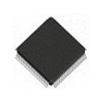
IDT72V3674L15PF IDT, Integrated Device Technology Inc, IDT72V3674L15PF Datasheet - Page 7

IDT72V3674L15PF
Manufacturer Part Number
IDT72V3674L15PF
Description
IC FIFO 16384X36 15NS 128QFP
Manufacturer
IDT, Integrated Device Technology Inc
Series
72Vr
Datasheet
1.IDT72V3654L15PF8.pdf
(37 pages)
Specifications of IDT72V3674L15PF
Function
Asynchronous
Memory Size
576K (16K x 36)
Data Rate
67MHz
Access Time
15ns
Voltage - Supply
3.15 V ~ 3.45 V
Operating Temperature
0°C ~ 70°C
Mounting Type
Surface Mount
Package / Case
128-TQFP, 128-VQFP
Configuration
Dual
Density
576Kb
Access Time (max)
10ns
Word Size
36b
Organization
8Kx36x2
Sync/async
Synchronous
Expandable
No
Bus Direction
Bi-Directional
Package Type
TQFP
Clock Freq (max)
66.7MHz
Operating Supply Voltage (typ)
3.3V
Operating Supply Voltage (min)
3.15V
Operating Supply Voltage (max)
3.45V
Supply Current
400mA
Operating Temp Range
0C to 70C
Operating Temperature Classification
Commercial
Mounting
Surface Mount
Pin Count
128
Lead Free Status / RoHS Status
Contains lead / RoHS non-compliant
Other names
72V3674L15PF
NOTE:
1. For 10ns speed grade: Vcc = 3.3V ± 0.15V, JEDEC JESD8-A compliant
ELECTRICAL CHARACTERISTICS OVER RECOMMENDED OPERATING FREE-
AIR TEMPERATURE RANGE (Unless otherwise noted)
NOTES:
1. Stresses beyond those listed under "Absolute Maximum Ratings" may cause permanent damage to the device. These are stress ratings only and functional operation of the device at these
2. The input and output voltage ratings may be exceeded provided the input and output current ratings are observed.
NOTES:
1. All typical values are at V
2. Commercial-10ns speed grade only: Vcc = 3.3V ± 0.15V, T
3. For additional I
4. Characterized values, not currently tested.
RECOMMENDED OPERATING CONDITIONS
ABSOLUTE MAXIMUM RATINGS OVER OPERATING FREE-AIR
TEMPERATURE RANGE (Unless otherwise noted)
IDT72V3654/72V3664/72V3674 3.3V CMOS SyncBiFIFO
2,048 x 36 x 2, 4,096 x 36 x 2 and 8,192 x 36 x 2
Symbol
Symbol
V
V
V
V
I
I
T
V
V
I
I
I
I
C
C
OH
LI
LO
CC2
CC3
OL
or any other conditions beyond those indicated under "recommended operating conditions" is not implied. Exposure to absolute-maximum-rated conditions for extended periods may affect
device reliability.
A
CC
CC
IH
IL
OH
OL
IN
OUT
Symbol
V
V
V
I
I
I
T
(4)
I
OK
OUT
CC
(1)
(3)
(3)
IK
CC
I
O
STG
(2)
(4)
(2)
Output Logic "1" Voltage
Output Logic "0" Voltage
Input Leakage Current (Any Input)
Output Leakage Current
Standby Current (with CLKA & CLKB running)
Standby Current (no clocks running)
Input Capacitance
Output Capacitance
Supply Voltage for 10ns
Supply Voltage for 15ns
High-Level Input Voltage
Low-Level Input Voltage
High-Level Output Current
Low-Level Output Current
Operating Temperature
CC
information, see Figure 1, Typical Characteristics: Supply Current (I
Parameter
Parameter
CC
= 3.3V, T
Supply Voltage Range
Input Voltage Range
Output Voltage Range
Input Clamp Current (V
Output Clamp Current (V
Continuous Output Current (V
Continuous Current Through V
Storage Temperature Range
A
= 25°C.
Min.
3.15
3.0
—
—
—
2
0
I
< 0 or V
O
A
V
V
V
V
V
V
V
V
= < 0 or V
Typ.
= 0° to +70°; JEDEC JESD8-A compliant.
3.3
3.3
CC
CC
CC
CC
CC
CC
I
O
—
—
—
—
—
= 0,
Rating
O
= 0,
CC
= 3.0V,
= 3.0V,
= 3.6V,
= 3.6V,
= 3.6V,
= 3.6V,
= 0 to V
I
> V
or GND
V
TM
CC
O
CC
Max.
3.45
3.6
0.8
WITH BUS-MATCHING
–4
70
> V
8
)
CC
+0.5
)
CC
)
I
I
V
V
V
V
f = 1 MHz
f = 1 MHZ
Test Conditions
OH
OL
7
Unit
I
O
I
I
mA
mA
°
= V
= V
= V
V
V
V
V
C
= V
= 8 mA
= –4 mA
CC
CC
CC
CC
) vs. Clock Frequency (f
CC
or 0
–0.2V or 0V
–0.2V or 0V
or 0
(1)
S
).
COMMERCIAL TEMPERATURE RANGE
–0.5 to V
–0.5 to V
Commercial
–0.5 to +4.6
–65 to 150
Min.
2.4
—
—
—
—
—
—
—
±400
±20
±50
±50
t
CLK
CC
CC
Commercial
IDT72V3654
IDT72V3664
IDT72V3674
+0.5
+0.5
= 10, 15 ns
Typ.
—
—
—
—
—
—
4
8
(1)
(2)
Max.
±10
±10
0.5
—
—
—
5
1
Unit
mA
mA
mA
mA
°C
Unit
V
V
V
mA
mA
µ A
µ A
pF
pF
V
V


