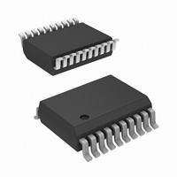
ISL55142IVZ Intersil, ISL55142IVZ Datasheet - Page 6

ISL55142IVZ
Manufacturer Part Number
ISL55142IVZ
Description
IC COMP CMOS HS 18V 20-TSSOP
Manufacturer
Intersil
Type
Windowr
Datasheet
1.ISL55141IVZ.pdf
(14 pages)
Specifications of ISL55142IVZ
Number Of Elements
2
Voltage - Supply
10 V ~ 18 V
Mounting Type
Surface Mount
Package / Case
20-TSSOP
Lead Free Status / RoHS Status
Lead free / RoHS Compliant
Test Circuits and Waveforms
Application Information
The ISL55141, ISL55142, ISL55143 provide 1, 2 and 4 dual
threshold, three-state window comparator(s) in TSSOP or
QFN footprints. They offer a combination of speed (10ns Tpd
and wide voltage range (18V). This product directly
addresses the need for unique common-mode
characteristics while supplying a power-down feature.
Figures 3 and 4 show the stimulus setup and measurement
points for an example propagation delay measurement.
Typical room temperature results are displayed in Figure 11.
Figure 4 shows a V
is increased in the horizontal axis from 50mV above and
below the reference (1.5V) up to 2.5V above and below the
1.5V reference.
Two lines are displayed in Figure 11. One represents the
rising-to-rising delay (t
falling-to-falling delay (t
Comparator Features
These three-state window comparators feature high output
current capability, and user defined high and low output levels
to interface with a wide variety of logic families. Each receiver
comprises two comparators and each comparator has an
independent threshold level input, making it easy to
implement (Minimum1-V
comparator functions. The CV
threshold levels of the A and B comparators respectively. V
and V
be more positive than V
supply pins, so the sources driving these pins must provide
adequate current for the expected load. V
typically connect to the power supplies of the logic device
driven by the comparator outputs.
FIGURE 3. t
V
OL
INP
CV
set all the comparator output levels, and V
CV
A
B
1.5V
1.5V
PD
INP
RECEIVER SWITCHING TEST CIRCUIT
+
-
-
+
PDLH
-3 V
range of 50mV. In Figure 11 the offset
+11 V
PDHL
OL
IH
EE
. These two inputs are unbuffered
)/(Maximum 0-V
CC
) and the other the
).
AX
6
+
and CV
5V-V
V
OL
OH
BX
OH
IL
(Continued)
pins set the
) logic level
ISL55141, ISL55142, ISL55143
and V
Q
Q
OL
OH
A
B
must
OH
The truth table for the receivers is given in Table 1. Receiver
outputs are not tri-statable, and do not incorporate any on-chip
short circuit current protection. Momentary short circuits to
GND, or any supply voltage, will not cause permanent
damage, but care must be taken to avoid longer duration short
circuits. If tolerable to the application, current limiting resistors
can be inserted in series with the Q
protect the receiver outputs from damage due to overcurrent
conditions.
Power-down Features
The ISL55141, ISL55142, ISL55143 PD pin provides a
means of reducing current consumption when the device is
not in use. Supply currents fall from ~7mA to less than 10µA
in the power-down mode. The device requires approximately
10µs to power-down and 15µs to power-up.
Power Supply Bypassing and Printed Circuit
Board Layout
As with any high frequency device, good printed circuit
board layout is necessary for optimum performance. Ground
plane construction is highly recommended, lead lengths
should be as short as possible, and the power supply pins
must be well bypassed to reduce the risk of oscillation. For
normal single supply operation, where the V
connected to ground, one 0.1µF ceramic capacitor should be
placed from the V
capacitor should then be connected from the V
ground. This same capacitor combination should be placed
at each supply pin to ground if split supplies are to be used.
Power Dissipation Considerations
Specifying continuous data rates, driver loads and driver
level amplitudes are key in determining power supply
requirements as well as dissipation/cooling necessities.
Driver output patterns also impact these needs. The faster
the pin activity, the greater the need to supply current and
remove heat.
V
INP
Q
FIGURE 4. t
CV
X
A
= CV
t
PDLH
B
= 1.5V
MEASUREMENT POINTS
PD
50%
RECEIVER PROPAGATION DELAY
CC
1.5V
pin to ground. A 4.7µF tantalum
AX
1.5V
and Q
50%
BX
EE
t
PDHL
CC
-50mV
outputs to
50mV
pin is
pin to
March 1, 2011
V
V
OH
OL
FN6230.2
(≈0V)
(≈5V)


