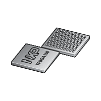
LPC1820FET100 NXP Semiconductors, LPC1820FET100 Datasheet - Page 76

LPC1820FET100
Manufacturer Part Number
LPC1820FET100
Description
The LPC1820FET100 is a high-performance, cost-effective Cortex-M3 microcontroller featuring 168 kB of SRAM, and advanced peripherals including High Speed USB 2
Manufacturer
NXP Semiconductors
Datasheet
1.LPC1810FBD144.pdf
(157 pages)
Available stocks
Company
Part Number
Manufacturer
Quantity
Price
Company:
Part Number:
LPC1820FET100
Manufacturer:
Signetics
Quantity:
45
- Current page: 76 of 157
- Download datasheet (3Mb)
NXP Semiconductors
LPC1850_30_20_10
Preliminary data sheet
7.13.2.1 Features
7.13.3 SPI Flash Interface (SPIFI)
example, a bidirectional port requires one stream for transmit and one for receives. The
source and destination areas can each be either a memory region or a peripheral for
master 1, but only memory for master 0.
The SPI Flash Interface (allows low-cost serial flash memories to be connected to the
ARM Cortex-M3 processor with little performance penalty compared to parallel flash
devices with higher pin count.
After a few commands configure the interface at startup, the entire flash content is
accessible as normal memory using byte, halfword, and word accesses by the processor
and/or DMA channels. Erasure and programming are handled by simple sequences of
commands.
Many serial flash devices use a half-duplex command-driven SPI protocol for device setup
and initialization and then move to a half-duplex, command-driven 4-bit protocol for
normal operation. Different serial flash vendors and devices accept or require different
•
•
•
•
•
•
•
•
•
•
•
•
•
•
•
•
Eight DMA channels. Each channel can support an unidirectional transfer.
16 DMA request lines.
Single DMA and burst DMA request signals. Each peripheral connected to the DMA
Controller can assert either a burst DMA request or a single DMA request. The DMA
burst size is set by programming the DMA Controller.
Memory-to-memory, memory-to-peripheral, peripheral-to-memory, and
peripheral-to-peripheral transfers are supported.
Scatter or gather DMA is supported through the use of linked lists. This means that
the source and destination areas do not have to occupy contiguous areas of memory.
Hardware DMA channel priority.
AHB slave DMA programming interface. The DMA Controller is programmed by
writing to the DMA control registers over the AHB slave interface.
Two AHB bus masters for transferring data. These interfaces transfer data when a
DMA request goes active. Master 1 can access memories and peripherals, master 0
can access memories only.
32-bit AHB master bus width.
Incrementing or non-incrementing addressing for source and destination.
Programmable DMA burst size. The DMA burst size can be programmed to more
efficiently transfer data.
Internal four-word FIFO per channel.
Supports 8, 16, and 32-bit wide transactions.
Big-endian and little-endian support. The DMA Controller defaults to little-endian
mode on reset.
An interrupt to the processor can be generated on a DMA completion or when a DMA
error has occurred.
Raw interrupt status. The DMA error and DMA count raw interrupt status can be read
prior to masking.
All information provided in this document is subject to legal disclaimers.
Rev. 3.1 — 15 December 2011
32-bit ARM Cortex-M3 microcontroller
LPC1850/30/20/10
© NXP B.V. 2011. All rights reserved.
76 of 157
Related parts for LPC1820FET100
Image
Part Number
Description
Manufacturer
Datasheet
Request
R
Part Number:
Description:
NXP Semiconductors designed the LPC2420/2460 microcontroller around a 16-bit/32-bitARM7TDMI-S CPU core with real-time debug interfaces that include both JTAG andembedded trace
Manufacturer:
NXP Semiconductors
Datasheet:

Part Number:
Description:
NXP Semiconductors designed the LPC2458 microcontroller around a 16-bit/32-bitARM7TDMI-S CPU core with real-time debug interfaces that include both JTAG andembedded trace
Manufacturer:
NXP Semiconductors
Datasheet:
Part Number:
Description:
NXP Semiconductors designed the LPC2468 microcontroller around a 16-bit/32-bitARM7TDMI-S CPU core with real-time debug interfaces that include both JTAG andembedded trace
Manufacturer:
NXP Semiconductors
Datasheet:
Part Number:
Description:
NXP Semiconductors designed the LPC2470 microcontroller, powered by theARM7TDMI-S core, to be a highly integrated microcontroller for a wide range ofapplications that require advanced communications and high quality graphic displays
Manufacturer:
NXP Semiconductors
Datasheet:
Part Number:
Description:
NXP Semiconductors designed the LPC2478 microcontroller, powered by theARM7TDMI-S core, to be a highly integrated microcontroller for a wide range ofapplications that require advanced communications and high quality graphic displays
Manufacturer:
NXP Semiconductors
Datasheet:
Part Number:
Description:
The Philips Semiconductors XA (eXtended Architecture) family of 16-bit single-chip microcontrollers is powerful enough to easily handle the requirements of high performance embedded applications, yet inexpensive enough to compete in the market for hi
Manufacturer:
NXP Semiconductors
Datasheet:
Part Number:
Description:
The XA-S3 device is a member of Philips Semiconductors? XA(eXtended Architecture) family of high performance 16-bitsingle-chip microcontrollers
Manufacturer:
NXP Semiconductors
Datasheet:

Part Number:
Description:
The NXP BlueStreak LH75401/LH75411 family consists of two low-cost 16/32-bit System-on-Chip (SoC) devices
Manufacturer:
NXP Semiconductors
Datasheet:

Part Number:
Description:
The NXP LPC3130/3131 combine an 180 MHz ARM926EJ-S CPU core, high-speed USB2
Manufacturer:
NXP Semiconductors
Datasheet:

Part Number:
Description:
The NXP LPC3141 combine a 270 MHz ARM926EJ-S CPU core, High-speed USB 2
Manufacturer:
NXP Semiconductors

Part Number:
Description:
The NXP LPC3143 combine a 270 MHz ARM926EJ-S CPU core, High-speed USB 2
Manufacturer:
NXP Semiconductors

Part Number:
Description:
The NXP LPC3152 combines an 180 MHz ARM926EJ-S CPU core, High-speed USB 2
Manufacturer:
NXP Semiconductors

Part Number:
Description:
The NXP LPC3154 combines an 180 MHz ARM926EJ-S CPU core, High-speed USB 2
Manufacturer:
NXP Semiconductors

Part Number:
Description:
Standard level N-channel enhancement mode Field-Effect Transistor (FET) in a plastic package using NXP High-Performance Automotive (HPA) TrenchMOS technology
Manufacturer:
NXP Semiconductors
Datasheet:


