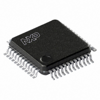
SC16C852LIB,157 NXP Semiconductors, SC16C852LIB,157 Datasheet - Page 10

SC16C852LIB,157
Manufacturer Part Number
SC16C852LIB,157
Description
IC UART DUAL W/FIFO 48-LQFP
Manufacturer
NXP Semiconductors
Datasheet
1.SC16C852LIBS151.pdf
(64 pages)
Specifications of SC16C852LIB,157
Features
Programmable
Number Of Channels
2, DUART
Fifo's
128 Byte
Protocol
RS485
Voltage - Supply
1.8V
With Auto Flow Control
Yes
With Irda Encoder/decoder
Yes
With False Start Bit Detection
Yes
With Modem Control
Yes
With Cmos
Yes
Mounting Type
Surface Mount
Package / Case
48-LQFP
Lead Free Status / RoHS Status
Lead free / RoHS Compliant
Other names
935283098157
SC16C852LIB
SC16C852LIB
SC16C852LIB
SC16C852LIB
Available stocks
Company
Part Number
Manufacturer
Quantity
Price
Company:
Part Number:
SC16C852LIB,157
Manufacturer:
NXP Semiconductors
Quantity:
10 000
NXP Semiconductors
Table 2.
SC16C852L
Product data sheet
Symbol
RXA
RXB
RXRDYA
RXRDYB
TXA
TXB
TXRDYA
TXRDYB
V
V
XTAL1
XTAL2
DD
SS
Pin description
Pin
LQFP48
5
4
31
18
7
8
43
6
42
17
13
14
HVQFN32 TFBGA36
4
3
-
-
5
6
-
-
26
13
10
11
[1]
…continued
D1
C2
-
-
D2
E1
-
-
C4
D4
F2
E3
All information provided in this document is subject to legal disclaimers.
1.8 V dual UART with 128-byte FIFOs and IrDA encoder/decoder
Type
I
I
O
O
O
O
O
O
I
I
I
O
Rev. 4 — 1 February 2011
Description
Receive data A, B. These inputs are associated with individual
serial channel data to the SC16C852L receive input circuits, A
through B. The RXx signal will be a logic 1 during reset, idle (no
data), or when not receiving data. During the local loopback mode,
the RXA/RXB input pin is disabled and transmit data is connected
to the UART receive input, internally.
Receive Ready A, B (active LOW). This function provides the
receive FIFO/RHR status for individual receive channels (A to B).
RXRDYx is primarily intended for monitoring DMA mode 1
transfers for the receive data FIFOs. A logic 0 indicates there is a
receive data to read/upload, that is, receive ready status with one
or more RX characters available in the FIFO/RHR. This pin is a
logic 1 when the FIFO/RHR is empty or when the programmed
trigger level has not been reached. This signal can also be used
for single mode transfers (DMA mode 0).
Transmit data A, B. These outputs are associated with individual
serial transmit channel data from the SC16C852L. The TXx signal
will be a logic 1 during reset, idle (no data), or when the transmitter
is disabled. During the local loopback mode, the TXA/TXB output
pin is disabled and transmit data is internally connected to the
UART receive input.
Transmit Ready A, B (active LOW). These outputs provide the
transmit FIFO/THR status for individual transmit channels (A to B).
TXRDYx is primarily intended for monitoring DMA mode 1
transfers for the transmit data FIFOs. An individual channel’s
TXRDYA, TXRDYB buffer ready status is indicated by logic 0, that
is, at lease one location is empty and available in the FIFO or THR.
This pin goes to a logic 1 (DMA mode 1) when there are no more
empty locations in the FIFO or THR. This signal can also be used
for single mode transfers (DMA mode 0).
Power supply input.
Signal and power ground.
Crystal or external clock input. Functions as a crystal input or as
an external clock input. A crystal can be connected between this
pin and XTAL2 to form an internal oscillator circuit. Alternatively, an
external clock can be connected to this pin to provide custom data
rates (see
See
Output of the crystal oscillator or buffered clock. (See also
XTAL1.) Crystal oscillator output or buffered clock output. Should
be left open if an external clock is connected to XTAL1.
Figure
Section 6.9 “Programmable baud rate
8.
SC16C852L
© NXP B.V. 2011. All rights reserved.
generator”).
10 of 64


