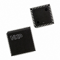
SC28L92A1A,512 NXP Semiconductors, SC28L92A1A,512 Datasheet - Page 39

SC28L92A1A,512
Manufacturer Part Number
SC28L92A1A,512
Description
IC UART DUAL W/FIFO 44-PLCC
Manufacturer
NXP Semiconductors
Series
IMPACTr
Datasheet
1.SC28L92A1B557.pdf
(73 pages)
Specifications of SC28L92A1A,512
Features
False-start Bit Detection
Number Of Channels
2, DUART
Fifo's
16 Byte
Voltage - Supply
3.3V, 5V
With Auto Flow Control
Yes
With False Start Bit Detection
Yes
With Modem Control
Yes
With Cmos
Yes
Mounting Type
Surface Mount
Package / Case
44-LCC (J-Lead)
Lead Free Status / RoHS Status
Lead free / RoHS Compliant
Other names
935263293512
SC28L92A1A
SC28L92A1A
SC28L92A1A
SC28L92A1A
Available stocks
Company
Part Number
Manufacturer
Quantity
Price
Company:
Part Number:
SC28L92A1A,512
Manufacturer:
NXP Semiconductors
Quantity:
10 000
NXP Semiconductors
SC28L92_7
Product data sheet
7.3.4.2 Status Register channel B (SRB)
7.3.5 Output Configuration Control Register (OPCR)
Table 43.
[1]
The bit definitions for this register are identical to the bit definitions for SRA, except that all
status applies to the channel B receiver and transmitter and the corresponding inputs and
outputs.
This register controls the signal presented by the OP[7:2] pins. The signal presented by
the OP[1:0] pins is controlled by the Rx, Tx, and the command register. The default
condition of the OP pins is to drive the complement of the data in the OPR[7:0] register.
When OP[7:2] pins drive DMA or interrupt type signals, they switch to open-drain
configuration. Otherwise, they drive strong logic 0 or logic 1 levels.
Table 44.
Table 45.
Bit
7
6
5
4
configure
received
break
OP7
These status bits are appended to the corresponding data character in the receive FIFO. A read of the
status provides these bits [7:5] from the top of the FIFO together with bits [4:0]. These bits are cleared by a
reset error status command. In character mode they are discarded when the corresponding data character
is read from the FIFO. In block error mode, the error-reset command (command 0x4 or receiver reset) must
used to clear block error conditions.
7
7
[1]
Symbol
-
-
-
-
SRB - Status register channel B (address 0x9) bit allocation
OPCR - Output configuration control register (address 0xD) bit allocation
OPCR - Output configuration control register (address 0xD) bit description
configure
framing
error
OP6
6
6
[1]
Description
OP7 output select
OP6 output select
OP5 output select
OP4 output select
Rev. 07 — 19 December 2007
0 = The complement of OPR[7]
1 = The channel B transmitter interrupt output which is the complement of
ISR[4]. When in this mode OP7 acts as an open-drain output. Note that
this output is not masked by the contents of the IMR.
0 = The complement of OPR[6]
1 = The channel A transmitter interrupt output which is the complement of
ISR[0]. When in this mode OP6 acts as an open-drain output. Note that
this output is not masked by the contents of the IMR.
0 = The complement of OPR[5]
1 = The channel B receiver interrupt output which is the complement of
ISR[5]. When in this mode OP5 acts as an open-drain output. Note that
this output is not masked by the contents of the IMR.
0 = The complement of OPR[4]
1 = The channel A receiver interrupt output which is the complement of
ISR[1]. When in this mode OP4 acts as an open-drain output. Note that
this output is not masked by the contents of the IMR.
3.3 V/5.0 V Dual Universal Asynchronous Receiver/Transmitter
configure
error
parity
OP5
5
5
[1]
overrun
configure
error
4
OP4
4
TxEMTB
3
configure OP3
3
TxRDYB
2
2
RxFULLB
SC28L92
© NXP B.V. 2007. All rights reserved.
1
configure OP2
1
RxRDYB
39 of 73
0
0


