SC28L92A1A,512 NXP Semiconductors, SC28L92A1A,512 Datasheet - Page 23

SC28L92A1A,512
Manufacturer Part Number
SC28L92A1A,512
Description
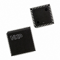
IC UART DUAL W/FIFO 44-PLCC
Manufacturer
NXP Semiconductors
Series
IMPACTr
Datasheet
1.SC28L92A1B557.pdf
(73 pages)
Specifications of SC28L92A1A,512
Features
False-start Bit Detection
Number Of Channels
2, DUART
Fifo's
16 Byte
Voltage - Supply
3.3V, 5V
With Auto Flow Control
Yes
With False Start Bit Detection
Yes
With Modem Control
Yes
With Cmos
Yes
Mounting Type
Surface Mount
Package / Case
44-LCC (J-Lead)
Lead Free Status / RoHS Status
Lead free / RoHS Compliant
Other names
935263293512
SC28L92A1A
SC28L92A1A
SC28L92A1A
SC28L92A1A
Available stocks
Company
Part Number
Manufacturer
Quantity
Price
Company:
Part Number:
SC28L92A1A,512
Manufacturer:
NXP Semiconductors
Quantity:
10 000
NXP Semiconductors
Table 4.
[1]
SC28L92_7
Product data sheet
Binary address
0
0
0
0
0
0
0
0
1
1
1
1
1
1
1
1
1
The three MR registers are accessed via the MR Pointer and Commands 0x1n and 0xBn (where n = represents receiver and transmitter
enable bits).
0
0
0
0
1
1
1
1
0
0
0
0
1
1
1
1
1
SC28L92 register addressing READ (RDN = 0), WRITE (WRN = 0)
0
0
1
1
0
0
1
1
0
0
1
1
0
0
0
1
1
0
1
0
1
0
1
0
1
0
1
0
1
0
0
1
0
1
For example, changing the number of bits per character while the transmitter is active may
cause the transmission of an incorrect character. In general, the contents of the MR, the
CSR, and the OPCR should only be changed while the receiver(s) and transmitter(s) are
not enabled, and certain changes to the ACR should only be made while the C/T is
stopped.
Each channel has three mode registers (MR0, MR1 and MR2) which control the basic
configuration of the channel. Access to these registers is controlled by independent MR
address pointers. These pointers are set to 0x0 or 0x1 by MR control commands in the
command register Miscellaneous Commands. Each time the MR registers are accessed
the MR pointer increments, stopping at MR2. It remains pointing to MR2 until set to 0x0 or
0x1 via the miscellaneous commands of the command register. The pointer is set to 0x1
on reset for compatibility with previous Philips Semiconductors UART software.
Mode, command, clock select, and status registers are duplicated for each channel to
provide total independent operation and control. Refer to
overview. The reserved registers at addresses 0x2 and 0xA should never be read during
normal operation since they are reserved for internal diagnostics.
Table 5.
Read operation (RDN = 0 and CEN = 0)
Mode Register A (MR0A, MR1A, MR2A)
Status Register A (SRA)
reserved
Rx Holding Register A (RxFIFOA)
Input Port Change Register (IPCR)
Interrupt Status Register (ISR)
Counter/Timer Upper (CTU)
Counter/Timer Lower (CTL)
Mode Register B (MR0B, MR1B, MR2B)
Status Register B (SRB)
reserved
Rx Holding Register B (RxFIFOB)
Interrupt vector (68xxx mode)
Miscellaneous register (Intel mode), IVR
Motorola mode
Input Port Register (IPR)
start counter command
stop counter command
Register name
Mode Register
Status Register
Clock Select
Registers for channels A and B
Rev. 07 — 19 December 2007
3.3 V/5.0 V Dual Universal Asynchronous Receiver/Transmitter
Channel A register
MRnA
SRA
CSRA
Write operation (WRN = 0 and CEN = 0)
Mode Register A (MR0A, MR1A, MR2A)
Clock Select Register A (CSRA)
Command Register A (CRA)
Tx Holding Register A (TxFIFOA)
Auxiliary Control Register (ACR)
Interrupt Mask Register (IMR)
C/T Upper Preset Register (CTPU)
C/T Lower Preset Register (CTPL)
Mode Register B (MR0B, MR1B, MR2B)
Clock Select Register B (CSRB)
Command Register B (CRB)
Tx Holding Register B (TxFIFOB)
Interrupt vector (68xxx mode)
Miscellaneous register (Intel mode), IVR
Motorola mode
Output Port Configuration Register (OPCR)
Set Output Port Bits Command (SOPR)
Reset output Port Bits Command (ROPR)
Channel B register
MRnB
SRB
CSRB
[1]
Section 7.2
Access
R/W
R only
W only
for register bit
SC28L92
© NXP B.V. 2007. All rights reserved.
23 of 73


