SC16C754BIBM,151 NXP Semiconductors, SC16C754BIBM,151 Datasheet - Page 6
SC16C754BIBM,151
Manufacturer Part Number
SC16C754BIBM,151
Description
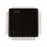
IC UART QUAD W/FIFO 64-LQFP
Manufacturer
NXP Semiconductors
Datasheet
1.SC16C754BIB80557.pdf
(51 pages)
Specifications of SC16C754BIBM,151
Number Of Channels
4, QUART
Package / Case
64-LQFP
Fifo's
64 Byte
Voltage - Supply
2.5V, 3.3V, 5V
With Auto Flow Control
Yes
With False Start Bit Detection
Yes
With Modem Control
Yes
Mounting Type
Surface Mount
Data Rate
5 Mbps
Supply Voltage (max)
5.5 V
Supply Voltage (min)
2.25 V
Supply Current
6 mA
Maximum Operating Temperature
+ 85 C
Minimum Operating Temperature
- 40 C
Mounting Style
SMD/SMT
Operating Supply Voltage
2.5 V or 3.3 V or 5 V
Lead Free Status / RoHS Status
Lead free / RoHS Compliant
Lead Free Status / RoHS Status
Lead free / RoHS Compliant, Lead free / RoHS Compliant
Other names
568-3290
935279069151
SC16C754BIBM-S
935279069151
SC16C754BIBM-S
Available stocks
Company
Part Number
Manufacturer
Quantity
Price
Company:

Part Number:
SC16C754BIBM,151
Manufacturer:
NXP Semiconductors
Quantity:
10 000


NXP Semiconductors
Table 2.
SC16C754B_4
Product data sheet
Symbol
A0
A1
A2
CDA
CDB
CDC
CDD
CLKSEL
Pin
LQFP64 LQFP80 PLCC68
24
23
22
64
18
31
49
-
Pin description
5.2 Pin description
30
29
28
79
23
39
63
26
Fig 4.
34
33
32
9
27
43
61
30
Pin configuration for PLCC68
DSRA
DTRA
DTRB
DSRB
CTSA
RTSA
RTSB
CTSB
INTA
INTB
GND
CSA
CSB
IOW
V
TXA
TXB
CC
Type
I
I
I
I
I
10
11
12
13
14
15
16
17
18
19
20
21
22
23
24
25
26
5 V, 3.3 V and 2.5 V quad UART, 5 Mbit/s (max.) with 64-byte FIFOs
Rev. 04 — 6 October 2008
Description
Address 0 select bit. Internal registers address selection.
Address 1 select bit. Internal registers address selection.
Address 2 select bit. Internal registers address selection.
Carrier Detect (active LOW). These inputs are associated with
individual UART channels A through D. A logic LOW on these pins
indicates that a carrier has been detected by the modem for that channel.
The state of these inputs is reflected in the Modem Status Register
(MSR).
Clock Select. CLKSEL selects the divide-by-1 or divide-by-4 prescalable
clock. During the reset, a logic 1 (V
divide-by-1 prescaler. A logic 0 (GND) on CLKSEL selects the divide-by-4
prescaler. The value of CLKSEL is latched into MCR[7] at the trailing
edge of RESET. A logic 1 (V
MCR[7]. A logic 0 (GND) on CLKSEL will latch a logic 1 into MCR[7].
MCR[7] can be changed after RESET to alter the prescaler value. This
pin is associated with LQFP80 and PLCC68 packages only. This pin is
connected to V
CC
SC16C754BIA68
internally on LQFP64 package.
CC
) on CLKSEL will latch a logic 0 into
CC
) on CLKSEL selects the
SC16C754B
002aaa868
60
59
58
57
56
55
54
53
52
51
50
49
48
47
46
45
44
© NXP B.V. 2008. All rights reserved.
DSRD
CTSD
DTRD
GND
RTSD
INTD
CSD
TXD
IOR
TXC
CSC
INTC
RTSC
V
DTRC
CTSC
DSRC
CC
6 of 51
Related parts for SC16C754BIBM,151
Image
Part Number
Description
Manufacturer
Datasheet
Request
R

Part Number:
Description:
5 V - 3.3 V and 2.5 V quad UART - 5 Mbit/s (max.)
Manufacturer:
NXP Semiconductors
Datasheet:
Part Number:
Description:
NXP Semiconductors designed the LPC2420/2460 microcontroller around a 16-bit/32-bitARM7TDMI-S CPU core with real-time debug interfaces that include both JTAG andembedded trace
Manufacturer:
NXP Semiconductors
Datasheet:

Part Number:
Description:
NXP Semiconductors designed the LPC2458 microcontroller around a 16-bit/32-bitARM7TDMI-S CPU core with real-time debug interfaces that include both JTAG andembedded trace
Manufacturer:
NXP Semiconductors
Datasheet:
Part Number:
Description:
NXP Semiconductors designed the LPC2468 microcontroller around a 16-bit/32-bitARM7TDMI-S CPU core with real-time debug interfaces that include both JTAG andembedded trace
Manufacturer:
NXP Semiconductors
Datasheet:
Part Number:
Description:
NXP Semiconductors designed the LPC2470 microcontroller, powered by theARM7TDMI-S core, to be a highly integrated microcontroller for a wide range ofapplications that require advanced communications and high quality graphic displays
Manufacturer:
NXP Semiconductors
Datasheet:
Part Number:
Description:
NXP Semiconductors designed the LPC2478 microcontroller, powered by theARM7TDMI-S core, to be a highly integrated microcontroller for a wide range ofapplications that require advanced communications and high quality graphic displays
Manufacturer:
NXP Semiconductors
Datasheet:
Part Number:
Description:
The Philips Semiconductors XA (eXtended Architecture) family of 16-bit single-chip microcontrollers is powerful enough to easily handle the requirements of high performance embedded applications, yet inexpensive enough to compete in the market for hi
Manufacturer:
NXP Semiconductors
Datasheet:
Part Number:
Description:
The XA-S3 device is a member of Philips Semiconductors? XA(eXtended Architecture) family of high performance 16-bitsingle-chip microcontrollers
Manufacturer:
NXP Semiconductors
Datasheet:

Part Number:
Description:
The NXP BlueStreak LH75401/LH75411 family consists of two low-cost 16/32-bit System-on-Chip (SoC) devices
Manufacturer:
NXP Semiconductors
Datasheet:
Part Number:
Description:
The NXP LPC3130/3131 combine an 180 MHz ARM926EJ-S CPU core, high-speed USB2
Manufacturer:
NXP Semiconductors
Datasheet:
Part Number:
Description:
The NXP LPC3141 combine a 270 MHz ARM926EJ-S CPU core, High-speed USB 2
Manufacturer:
NXP Semiconductors
Part Number:
Description:
The NXP LPC3143 combine a 270 MHz ARM926EJ-S CPU core, High-speed USB 2
Manufacturer:
NXP Semiconductors

Part Number:
Description:
The NXP LPC3152 combines an 180 MHz ARM926EJ-S CPU core, High-speed USB 2
Manufacturer:
NXP Semiconductors
Part Number:
Description:
The NXP LPC3154 combines an 180 MHz ARM926EJ-S CPU core, High-speed USB 2
Manufacturer:
NXP Semiconductors