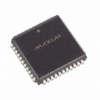
DS2151QB Maxim Integrated Products, DS2151QB Datasheet - Page 19

DS2151QB
Manufacturer Part Number
DS2151QB
Description
IC TXRX T1 1-CHIP 5V LP 44-PLCC
Manufacturer
Maxim Integrated Products
Datasheet
1.DS2151QB.pdf
(60 pages)
Specifications of DS2151QB
Function
Single-Chip Transceiver
Interface
T1
Number Of Circuits
1
Voltage - Supply
4.75 V ~ 5.25 V
Current - Supply
65mA
Operating Temperature
0°C ~ 70°C
Mounting Type
Surface Mount
Package / Case
44-LCC, 44-PLCC
Includes
Alarm Detector and Generator, CSU Loop Codes Generator and Detector, DSX-1 and CSU Line Build-Outs Generator
Lead Free Status / RoHS Status
Contains lead / RoHS non-compliant
Power (watts)
-
Available stocks
Company
Part Number
Manufacturer
Quantity
Price
Part Number:
DS2151QB
Manufacturer:
DALLAS
Quantity:
20 000
Company:
Part Number:
DS2151QB+
Manufacturer:
Maxim Integrated Products
Quantity:
135
Company:
Part Number:
DS2151QB+
Manufacturer:
VISHAY
Quantity:
6 509
DS2151Q
5 STATUS AND INFORMATION REGISTERS
There is a set of four registers that contain information on the current real time status of the DS2151Q:
Status Register 1 (SR1), Status Register 2 (SR2), Receive Information Register 1 (RIR1), and Receive
Information Register 2 (RIR2). When a particular event has occurred (or is occurring), the appropriate bit
in one of these four registers will be set to a 1. All of the bits in these registers operate in a latched
fashion. This means that if an event occurs and a bit is set to a 1 in any of the registers, it will remain set
until the user reads that bit. The bit will be cleared when it is read and it will not be set again until the
event has occurred again or if the alarm(s) is still present.
The user will always precede a read of these registers with a write. The byte written to the register will
inform the DS2151Q which bits the user wishes to read and have cleared. The user will write a byte to
one of these four registers, with a 1 in the bit positions he or she wishes to read and a 0 in the bit positions
he or she does not wish to obtain the latest information on. When a 1 is written to a bit location, the read
register will be updated with current value and the previous value will be cleared. When a 0 is written to a
bit position, the read register will not be updated and the previous value will be held. A write to the status
and information registers will be immediately followed by a read of the same register. The read result
should be logically ANDed with the mask byte that was just written and this value should be written back
into the same register to ensure that the bit does indeed clear. This second write is necessary because the
alarms and events in the status registers occur asynchronously in respect to their access via the parallel
port. The write-read-write scheme is unique to the four status registers and it allows an external
microcontroller or microprocessor to individually poll certain bits without disturbing the other bits in the
register. This operation is key in controlling the DS2151Q with higher-order software languages.
The SR1 and SR2 registers have the unique ability to initiate a hardware interrupt via the
and
INT1
INT2
pins, respectively. Each of the alarms and events in the SR1 and SR2 can be either masked or unmasked
from the interrupt pins via the Interrupt Mask Register 1 (IMR1) and Interrupt Mask Register 2 (IMR2)
respectively.
19 of 60


