DS2151QB+ Maxim Integrated Products, DS2151QB+ Datasheet - Page 7
DS2151QB+
Manufacturer Part Number
DS2151QB+
Description
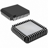
IC TXRX T1 1-CHIP 5V LP 44-PLCC
Manufacturer
Maxim Integrated Products
Datasheet
1.DS2151QB.pdf
(60 pages)
Specifications of DS2151QB+
Function
Single-Chip Transceiver
Interface
T1
Number Of Circuits
1
Voltage - Supply
4.75 V ~ 5.25 V
Current - Supply
65mA
Operating Temperature
0°C ~ 70°C
Mounting Type
Surface Mount
Package / Case
44-LCC, 44-PLCC
Includes
Alarm Detector and Generator, CSU Loop Codes Generator and Detector, DSX-1 and CSU Line Build-Outs Generator
Lead Free Status / RoHS Status
Lead free / RoHS Compliant
Power (watts)
-


21, 22
25, 26
PIN
20
23
24
27
28
29
30
31
32
33
34
35
36
37
38
39
40
TCHBLK
TCHCLK
XTAL1,
TSYNC
XTAL2
TLCLK
NAME
RRING
TRING
TLINK
DVDD
RVDD
TVDD
TCLK
RVSS
RTIP,
TVSS
TSER
INT1
INT2
TTIP
BTS
TYPE
I/O
—
—
—
—
—
—
—
—
—
O
O
O
O
O
I
I
I
I
Bus Type Select. Strap high to select Motorola bus timing; strap low to select
Intel bus timing. This pin controls the function of the RD(DS), ALE(AS), and
WR(R/W) pins. If BTS = 1, then these pins assume the function listed in
parentheses.
Receive Tip and Ring. Analog inputs for clock recovery circuitry; connects
to a 1:1 transformer (see Section
Receive Analog Positive Supply. 5.0V. Should be tied to DVDD and TVDD
pins.
Receive Signal Ground. 0V. Should be tied to local ground plane.
Crystal Connections. A pullable 6.176MHz crystal must be applied to these
pins. See Section
Receive Alarm Interrupt 1. Flags host controller during alarm conditions
defined in Status Register 1. Active low, open drain output.
Receive Alarm Interrupt 2. Flags host controller during conditions defined
in Status Register 2. Active low, open drain output.
Transmit Tip. Analog line driver output; connects to a step-up transformer
(see Section
Transmit Signal Ground. 0V. Should be tied to local ground plane.
Transmit Analog Positive Supply. 5.0V. Should be tied to DVDD and
RVDD pins.
Transmit Ring. Analog line driver outputs; connects to a step-up transformer
(see Section
Transmit Channel Block. A user-programmable output that can be forced
high or low during any of the 24 T1 channels. Useful for blocking clocks to a
serial UART or LAPD controller in applications where not all T1 channels are
used such as Fractional T1, 384kbps service, 768kbps, or ISDN-PRI. Also
useful for locating individual channels in drop-and-insert applications. See
Section
Transmit Link Clock. 4kHz or 2kHz (ZBTSI) demand clock for the TLINK
input. See Section
Transmit Link Data. If enabled via TCR1.2, this pin will be sampled during
the F-bit time on the falling edge of TCLK for data insertion into either the
FDL stream (ESF) or the Fs bit position (D4) or the Z-bit position (ZBTSI).
See Section
Transmit Sync. A pulse at this pin will establish either frame or multiframe
boundaries for the DS2151Q. Via TCR2.2, the DS2151Q can be programmed
to output either a frame or multiframe pulse at this pin. If this pin is set to
output pulses at frame boundaries, it can also be set via TCR2.4 to output
double-wide pulses at signaling frames. See Section
Digital Positive Supply. 5.0V. Should be tied to RVDD and TVDD pins.
Transmit Clock. 1.544MHz primary clock.
Transmit Serial Data. Transmit NRZ serial data, sampled on the falling edge
of TCLK.
Transmit Channel Clock. 192kHz clock that pulses high during the LSB of
each channel. Useful for parallel to serial conversion of channel data, locating
robbed-bit signaling bits, and for blocking clocks in DDS applications. See
Section
14
14
for timing details.
for timing details.
14
13
13
for timing details.
for details).
for details).
13
14
7 of 60
for crystal specifications.
for timing details.
FUNCTION
13
for details).
14
for timing details.
Related parts for DS2151QB+
Image
Part Number
Description
Manufacturer
Datasheet
Request
R

Part Number:
Description:
MAX7528KCWPMaxim Integrated Products [CMOS Dual 8-Bit Buffered Multiplying DACs]
Manufacturer:
Maxim Integrated Products
Datasheet:
Part Number:
Description:
Single +5V, fully integrated, 1.25Gbps laser diode driver.
Manufacturer:
Maxim Integrated Products
Datasheet:
Part Number:
Description:
Single +5V, fully integrated, 155Mbps laser diode driver.
Manufacturer:
Maxim Integrated Products
Datasheet:
Part Number:
Description:
VRD11/VRD10, K8 Rev F 2/3/4-Phase PWM Controllers with Integrated Dual MOSFET Drivers
Manufacturer:
Maxim Integrated Products
Datasheet:
Part Number:
Description:
Highly Integrated Level 2 SMBus Battery Chargers
Manufacturer:
Maxim Integrated Products
Datasheet:
Part Number:
Description:
Current Monitor and Accumulator with Integrated Sense Resistor; ; Temperature Range: -40°C to +85°C
Manufacturer:
Maxim Integrated Products
Part Number:
Description:
TSSOP 14/A�/RS-485 Transceivers with Integrated 100O/120O Termination Resis
Manufacturer:
Maxim Integrated Products
Part Number:
Description:
TSSOP 14/A�/RS-485 Transceivers with Integrated 100O/120O Termination Resis
Manufacturer:
Maxim Integrated Products
Part Number:
Description:
QFN 16/A�/AC-DC and DC-DC Peak-Current-Mode Converters with Integrated Step
Manufacturer:
Maxim Integrated Products
Part Number:
Description:
TDFN/A/65V, 1A, 600KHZ, SYNCHRONOUS STEP-DOWN REGULATOR WITH INTEGRATED SWI
Manufacturer:
Maxim Integrated Products
Part Number:
Description:
Integrated Temperature Controller f
Manufacturer:
Maxim Integrated Products
Part Number:
Description:
SOT23-6/I�/45MHz to 650MHz, Integrated IF VCOs with Differential Output
Manufacturer:
Maxim Integrated Products
Part Number:
Description:
SOT23-6/I�/45MHz to 650MHz, Integrated IF VCOs with Differential Output
Manufacturer:
Maxim Integrated Products
Part Number:
Description:
EVALUATION KIT/2.4GHZ TO 2.5GHZ 802.11G/B RF TRANSCEIVER WITH INTEGRATED PA
Manufacturer:
Maxim Integrated Products
Part Number:
Description:
QFN/E/DUAL PCIE/SATA HIGH SPEED SWITCH WITH INTEGRATED BIAS RESISTOR
Manufacturer:
Maxim Integrated Products
Datasheet: