DS2151QB+ Maxim Integrated Products, DS2151QB+ Datasheet - Page 4
DS2151QB+
Manufacturer Part Number
DS2151QB+
Description
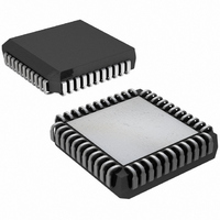
IC TXRX T1 1-CHIP 5V LP 44-PLCC
Manufacturer
Maxim Integrated Products
Datasheet
1.DS2151QB.pdf
(60 pages)
Specifications of DS2151QB+
Function
Single-Chip Transceiver
Interface
T1
Number Of Circuits
1
Voltage - Supply
4.75 V ~ 5.25 V
Current - Supply
65mA
Operating Temperature
0°C ~ 70°C
Mounting Type
Surface Mount
Package / Case
44-LCC, 44-PLCC
Includes
Alarm Detector and Generator, CSU Loop Codes Generator and Detector, DSX-1 and CSU Line Build-Outs Generator
Lead Free Status / RoHS Status
Lead free / RoHS Compliant
Power (watts)
-


DS2151Q
1 DETAILED DESCRIPTION
The DS2151Q T1 single-chip transceiver (SCT) contains all the necessary functions for connection to T1
lines whether they be DS-1 long haul or DSX-1 short haul. The clock recovery circuitry automatically
adjusts to T1 lines from 0 feet to over 6000 feet in length. The device can generate both DSX-1 line
build-outs as well as CSU build-outs of -7.5dB, -15dB, and -22.5dB. The on-board jitter attenuator
(selectable to either 32 bits or 128 bits) can be placed in either the transmit or receive data paths. The
framer locates the frame and multiframe boundaries and monitors the data stream for alarms. It is also
used for extracting and inserting robbed-bit signaling data and FDL data. The device contains a set of 64
8-bit internal registers that the user can access to control the operation of the unit. Quick access via the
parallel control port allows a single micro to handle many T1 lines. The device fully meets all of the latest
T1 specifications including ANSI T1.403-199X, AT&T TR 62411 (12-90), and ITU G.703, G.704,
G.706, G.823, and I.431.
1.1 Introduction
The analog AMI waveform off of the T1 line is transformer coupled into the RRING and RTIP pins of
the DS2151Q. The device recovers clock and data from the analog signal and passes it through the jitter
attenuation mux to the receive side framer where the digital serial stream is analyzed to locate the framing
pattern. If needed, the receive side elastic store can be enabled in order to absorb the phase and frequency
differences between the recovered T1 data stream and an asynchronous backplane clock which is
provided at the SYSCLK input.
The transmit side of the DS2151Q is totally independent from the receive side in both the clock
requirements and characteristics. Data can be either provided directly to the transmit formatter or via an
elastic store. The transmit formatter will provide the necessary data overhead for T1 transmission. Once
the data stream has been prepared for transmission, it is sent via the jitter attenuation mux to the
waveshaping and line driver functions. The DS2151Q will drive the T1 line from the TTIP and TRING
pins via a coupling transformer.
4 of 60
Related parts for DS2151QB+
Image
Part Number
Description
Manufacturer
Datasheet
Request
R

Part Number:
Description:
MAX7528KCWPMaxim Integrated Products [CMOS Dual 8-Bit Buffered Multiplying DACs]
Manufacturer:
Maxim Integrated Products
Datasheet:
Part Number:
Description:
Single +5V, fully integrated, 1.25Gbps laser diode driver.
Manufacturer:
Maxim Integrated Products
Datasheet:
Part Number:
Description:
Single +5V, fully integrated, 155Mbps laser diode driver.
Manufacturer:
Maxim Integrated Products
Datasheet:
Part Number:
Description:
VRD11/VRD10, K8 Rev F 2/3/4-Phase PWM Controllers with Integrated Dual MOSFET Drivers
Manufacturer:
Maxim Integrated Products
Datasheet:
Part Number:
Description:
Highly Integrated Level 2 SMBus Battery Chargers
Manufacturer:
Maxim Integrated Products
Datasheet:
Part Number:
Description:
Current Monitor and Accumulator with Integrated Sense Resistor; ; Temperature Range: -40°C to +85°C
Manufacturer:
Maxim Integrated Products
Part Number:
Description:
TSSOP 14/A�/RS-485 Transceivers with Integrated 100O/120O Termination Resis
Manufacturer:
Maxim Integrated Products
Part Number:
Description:
TSSOP 14/A�/RS-485 Transceivers with Integrated 100O/120O Termination Resis
Manufacturer:
Maxim Integrated Products
Part Number:
Description:
QFN 16/A�/AC-DC and DC-DC Peak-Current-Mode Converters with Integrated Step
Manufacturer:
Maxim Integrated Products
Part Number:
Description:
TDFN/A/65V, 1A, 600KHZ, SYNCHRONOUS STEP-DOWN REGULATOR WITH INTEGRATED SWI
Manufacturer:
Maxim Integrated Products
Part Number:
Description:
Integrated Temperature Controller f
Manufacturer:
Maxim Integrated Products
Part Number:
Description:
SOT23-6/I�/45MHz to 650MHz, Integrated IF VCOs with Differential Output
Manufacturer:
Maxim Integrated Products
Part Number:
Description:
SOT23-6/I�/45MHz to 650MHz, Integrated IF VCOs with Differential Output
Manufacturer:
Maxim Integrated Products
Part Number:
Description:
EVALUATION KIT/2.4GHZ TO 2.5GHZ 802.11G/B RF TRANSCEIVER WITH INTEGRATED PA
Manufacturer:
Maxim Integrated Products
Part Number:
Description:
QFN/E/DUAL PCIE/SATA HIGH SPEED SWITCH WITH INTEGRATED BIAS RESISTOR
Manufacturer:
Maxim Integrated Products
Datasheet: