DS2151QB+ Maxim Integrated Products, DS2151QB+ Datasheet - Page 3
DS2151QB+
Manufacturer Part Number
DS2151QB+
Description
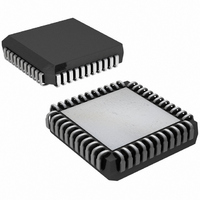
IC TXRX T1 1-CHIP 5V LP 44-PLCC
Manufacturer
Maxim Integrated Products
Datasheet
1.DS2151QB.pdf
(60 pages)
Specifications of DS2151QB+
Function
Single-Chip Transceiver
Interface
T1
Number Of Circuits
1
Voltage - Supply
4.75 V ~ 5.25 V
Current - Supply
65mA
Operating Temperature
0°C ~ 70°C
Mounting Type
Surface Mount
Package / Case
44-LCC, 44-PLCC
Includes
Alarm Detector and Generator, CSU Loop Codes Generator and Detector, DSX-1 and CSU Line Build-Outs Generator
Lead Free Status / RoHS Status
Lead free / RoHS Compliant
Power (watts)
-


DS2151Q
LIST OF FIGURES
Figure 1-1. DS2151Q Block Diagram ......................................................................................................... 5
Figure 13-1. External Analog Connections............................................................................................... 43
Figure 13-2. Jitter Tolerance .................................................................................................................... 43
Figure 13-3. Transmit Waveform Template .............................................................................................. 44
Figure 13-4. Jitter Attenuation .................................................................................................................. 45
Figure 14-1. Receive Side D4 Timing....................................................................................................... 46
Figure 14-2. Receive Side ESF Timing .................................................................................................... 46
Figure 14-3. Receive Side Boundary Timing with Elastic Store(s) Disabled ............................................ 47
Figure 14-4. 1.544MHz Boundary Timing with Elastic Store(s) Enabled.................................................. 47
Figure 14-5. 2.048MHz Boundary Timing with Elastic Store(s) Enabled.................................................. 48
Figure 14-6. Transmit Side D4 Timing...................................................................................................... 48
Figure 14-7. Transmit Side ESF Timing ................................................................................................... 49
Figure 14-8. Transmit Side Boundary Timing with Elastic Store(s) Disabled ........................................... 50
Figure 14-9. Transmit Data Flow .............................................................................................................. 51
Figure 16-1. Intel Bus Read AC Timing.................................................................................................... 54
Figure 16-2. Intel Bus Write AC Timing .................................................................................................... 54
Figure 16-3. Motorola Bus AC Timing ...................................................................................................... 55
Figure 16-4. Receive Side AC Timing ...................................................................................................... 57
Figure 16-5. Transmit Side AC Timing ..................................................................................................... 59
LIST OF TABLES
Table 4-1. Output Pin Test Modes............................................................................................................ 13
Table 5-1. Receive T1 Level Indication .................................................................................................... 21
Table 5-2. Alarm Set and Clear Criteria ................................................................................................... 23
Table 6-1. Line Code Violation Counting Arrangements .......................................................................... 27
Table 6-2. Path Code Violation Counting Arrangements.......................................................................... 28
Table 6-3. Multiframes Out of Sync Counting Arrangements ................................................................... 29
Table 13-1. Source of RCLK Upon RCL................................................................................................... 40
Table 13-2. LBO Select in LICR ............................................................................................................... 41
Table 13-3. Transformer Specifications.................................................................................................... 41
Table 13-4. Crystal Selection Guidelines ................................................................................................. 42
Table 15-1. Recommended DC Characteristics ....................................................................................... 52
Table 15-2. Capacitance .......................................................................................................................... 52
Table 15-3. DC Characteristics ................................................................................................................ 52
Table 16-1. AC Characteristics—Parallel Port ......................................................................................... 53
Table 16-2. AC Characteristics—Receive Side ........................................................................................ 56
Table 16-3. AC Characteristics—Transmit Side ....................................................................................... 58
3 of 60
Related parts for DS2151QB+
Image
Part Number
Description
Manufacturer
Datasheet
Request
R

Part Number:
Description:
MAX7528KCWPMaxim Integrated Products [CMOS Dual 8-Bit Buffered Multiplying DACs]
Manufacturer:
Maxim Integrated Products
Datasheet:
Part Number:
Description:
Single +5V, fully integrated, 1.25Gbps laser diode driver.
Manufacturer:
Maxim Integrated Products
Datasheet:
Part Number:
Description:
Single +5V, fully integrated, 155Mbps laser diode driver.
Manufacturer:
Maxim Integrated Products
Datasheet:
Part Number:
Description:
VRD11/VRD10, K8 Rev F 2/3/4-Phase PWM Controllers with Integrated Dual MOSFET Drivers
Manufacturer:
Maxim Integrated Products
Datasheet:
Part Number:
Description:
Highly Integrated Level 2 SMBus Battery Chargers
Manufacturer:
Maxim Integrated Products
Datasheet:
Part Number:
Description:
Current Monitor and Accumulator with Integrated Sense Resistor; ; Temperature Range: -40°C to +85°C
Manufacturer:
Maxim Integrated Products
Part Number:
Description:
TSSOP 14/A�/RS-485 Transceivers with Integrated 100O/120O Termination Resis
Manufacturer:
Maxim Integrated Products
Part Number:
Description:
TSSOP 14/A�/RS-485 Transceivers with Integrated 100O/120O Termination Resis
Manufacturer:
Maxim Integrated Products
Part Number:
Description:
QFN 16/A�/AC-DC and DC-DC Peak-Current-Mode Converters with Integrated Step
Manufacturer:
Maxim Integrated Products
Part Number:
Description:
TDFN/A/65V, 1A, 600KHZ, SYNCHRONOUS STEP-DOWN REGULATOR WITH INTEGRATED SWI
Manufacturer:
Maxim Integrated Products
Part Number:
Description:
Integrated Temperature Controller f
Manufacturer:
Maxim Integrated Products
Part Number:
Description:
SOT23-6/I�/45MHz to 650MHz, Integrated IF VCOs with Differential Output
Manufacturer:
Maxim Integrated Products
Part Number:
Description:
SOT23-6/I�/45MHz to 650MHz, Integrated IF VCOs with Differential Output
Manufacturer:
Maxim Integrated Products
Part Number:
Description:
EVALUATION KIT/2.4GHZ TO 2.5GHZ 802.11G/B RF TRANSCEIVER WITH INTEGRATED PA
Manufacturer:
Maxim Integrated Products
Part Number:
Description:
QFN/E/DUAL PCIE/SATA HIGH SPEED SWITCH WITH INTEGRATED BIAS RESISTOR
Manufacturer:
Maxim Integrated Products
Datasheet: