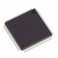
DS2156L+ Maxim Integrated Products, DS2156L+ Datasheet - Page 182

DS2156L+
Manufacturer Part Number
DS2156L+
Description
IC TXRX T1/E1/J1 1-CHIP 100-LQFP
Manufacturer
Maxim Integrated Products
Datasheet
1.DS2156L.pdf
(265 pages)
Specifications of DS2156L+
Function
Single-Chip Transceiver
Interface
E1, J1, T1, TDM, UTOPIA II
Number Of Circuits
1
Voltage - Supply
3.14 V ~ 3.47 V
Current - Supply
75mA
Operating Temperature
0°C ~ 70°C
Mounting Type
Surface Mount
Package / Case
100-LQFP
Includes
BERT Generator and Detector, CMI Coder and Decoder, HDLC Controller
Lead Free Status / RoHS Status
Lead free / RoHS Compliant
Power (watts)
-
- Current page: 182 of 265
- Download datasheet (2Mb)
24.7 Register Definitions
The CCR2 register is used to configure the UTOPIA port address. The upper five bits of the CCR2
register contain the port address 0–31. The lower three bits are used for the backplane clock function. See
Programmable Backplane Clock Synthesizer in Section 30.
Register Name:
Register Description:
Register Address:
Bit #
Name
Default
Bit 0/BPEN. See Section 30 for more information.
Bit 1/BPCS0. See Section 30 for more information.
Bit 2/BPCS1. See Section 30 for more information.
Bits 3 to 7/Transmit and Receive Port Address 0 to 4 (TRPA0 to TRPA4). The 5-bit value in this register is
used to assign the UTOPIA interface 1 of 32 port addresses.
Register Name:
Register Description:
Register Address:
Bit #
Name
Default
Bit 0/Transmit Port Configuration (TPC)
Bit 1/Transmit Poll Mode (TPM). Transmit UTOPIA polling mode configuration
Bits 2 to 7/Unassigned, must be set to 0 for proper operation
0 = T1 mode
1 = E1 mode
0 = multiplexed with 1CLAV mode
1 = direct status
TRPA4
—
7
7
0
0
TRPA3
—
CCR2
Common Control Register 2
71h
U_TCFR
UTOPIA Transmit Configuration Register
50h
6
0
6
0
TRPA2
—
5
0
5
0
TRPA1
—
4
0
4
1
182 of 265
TRPA0
—
3
0
3
0
BPCS1
—
2
0
2
0
BPCS0
TPM
1
0
1
0
BPEN
TPC
0
0
0
0
Related parts for DS2156L+
Image
Part Number
Description
Manufacturer
Datasheet
Request
R

Part Number:
Description:
Ds2156, Ds2156l, Ds2156ln T1/e1/j1 Single-chip Transceiver Tdm/utopia Ii Interface
Manufacturer:
Maxim Integrated Products, Inc.
Datasheet:

Part Number:
Description:
MAX7528KCWPMaxim Integrated Products [CMOS Dual 8-Bit Buffered Multiplying DACs]
Manufacturer:
Maxim Integrated Products
Datasheet:

Part Number:
Description:
Single +5V, fully integrated, 1.25Gbps laser diode driver.
Manufacturer:
Maxim Integrated Products
Datasheet:

Part Number:
Description:
Single +5V, fully integrated, 155Mbps laser diode driver.
Manufacturer:
Maxim Integrated Products
Datasheet:

Part Number:
Description:
VRD11/VRD10, K8 Rev F 2/3/4-Phase PWM Controllers with Integrated Dual MOSFET Drivers
Manufacturer:
Maxim Integrated Products
Datasheet:

Part Number:
Description:
Highly Integrated Level 2 SMBus Battery Chargers
Manufacturer:
Maxim Integrated Products
Datasheet:

Part Number:
Description:
Current Monitor and Accumulator with Integrated Sense Resistor; ; Temperature Range: -40°C to +85°C
Manufacturer:
Maxim Integrated Products

Part Number:
Description:
TSSOP 14/A�/RS-485 Transceivers with Integrated 100O/120O Termination Resis
Manufacturer:
Maxim Integrated Products

Part Number:
Description:
TSSOP 14/A�/RS-485 Transceivers with Integrated 100O/120O Termination Resis
Manufacturer:
Maxim Integrated Products

Part Number:
Description:
QFN 16/A�/AC-DC and DC-DC Peak-Current-Mode Converters with Integrated Step
Manufacturer:
Maxim Integrated Products

Part Number:
Description:
TDFN/A/65V, 1A, 600KHZ, SYNCHRONOUS STEP-DOWN REGULATOR WITH INTEGRATED SWI
Manufacturer:
Maxim Integrated Products

Part Number:
Description:
Integrated Temperature Controller f
Manufacturer:
Maxim Integrated Products

Part Number:
Description:
SOT23-6/I�/45MHz to 650MHz, Integrated IF VCOs with Differential Output
Manufacturer:
Maxim Integrated Products

Part Number:
Description:
SOT23-6/I�/45MHz to 650MHz, Integrated IF VCOs with Differential Output
Manufacturer:
Maxim Integrated Products

Part Number:
Description:
EVALUATION KIT/2.4GHZ TO 2.5GHZ 802.11G/B RF TRANSCEIVER WITH INTEGRATED PA
Manufacturer:
Maxim Integrated Products


