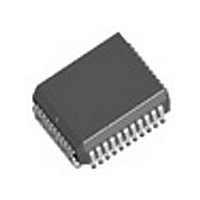
TXC02050AIPL Transwitch Corporation, TXC02050AIPL Datasheet - Page 2

TXC02050AIPL
Manufacturer Part Number
TXC02050AIPL
Description
Manufacturer
Transwitch Corporation
Datasheet
1.TXC02050AIPL.pdf
(26 pages)
Specifications of TXC02050AIPL
Operating Temperature (min)
-40C
Operating Temperature Classification
Industrial
Operating Temperature (max)
85C
Package Type
PLCC
Rad Hardened
No
Lead Free Status / Rohs Status
Not Compliant
BLOCK DIAGRAM
BLOCK DIAGRAM DESCRIPTION
On the Line Side, a symmetrical bipolar signal is applied to the input signal pin (DI1), which requires an exter-
nal 75 termination. DI2 is a DC reference voltage output which serves as an AC ground.
Equalization for various lengths of cable having a f characteristic is compensated by the two EQB0 and
EQB1 signal leads. The Equalization Network Block is connected to an AGC Block which has approximately a
20 dB dynamic range. The AGC has separate voltage and ground leads for noise immunity, and uses an exter-
nal capacitor as part of an AGC filter. The AGC output is connected to the Clock Recovery Block.
The Clock Recovery Block contains a phase-locked loop and supporting logic to generate a clock signal from
the line signal. The signal lead LOW selects the appropriate circuit in the Clock Recovery Block for the operat-
ing frequency and provides input attenuation for the receive line signal. The line signal is monitored for loss of
signal, with an alarm indication provided on the RXLOS signal lead. The Clock Recovery Block requires an
external reference clock at the operating frequency (DCK). The reference clock is also used for generating and
sending a receive Alarm Indication Signal (AIS). The generation and sending of AIS for recovered data is con-
trolled by the RXAIS signal lead.
The output of the Clock Recovery Block is connected to the HDB3 Decoder Block or the Output Circuits Block.
When the decoder is enabled, indications of coding violation errors, other than the normal HDB3 zero substitu-
tion codes, are provided as pulses on the signal lead labeled CV. An external clock (BERCK) is used to gener-
ate a 10-second sampling window for detecting a 10
provided on the signal lead labeled LQLTY.
LBKTX
TNO
TPO
DI1
DI2
LINE
SIDE
EQB1
VDD
Equalization
Network
EQB0
GND
LOW
VAGC
AGC
Output
Driver
GNDA
AGFIL
Figure 1. MRT Block Diagram
VCOC
Recovery
Clock
RXLOS
DCK
PLLC
clk
+
-
- 2 -
-6
Encoder
LBKRX
HDB3
Decoder
or greater error rate. The line quality indication is
HDB3
PNENB
BERCK
Detector
Error
CV
CV
LQLTY
DCK
clk
+
-
clk
+
-
TERMINAL
TXAIS
RXDIS
Circuits
I/O
SIDE
TXLOC
RXAIS
Ed. 3, April 1994
TXC-02050-MB
RP/RD
RN
CLKO
CLKO
TP/TD
TN
CLKI
MRT


