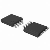
74HC2G66DP,125 NXP Semiconductors, 74HC2G66DP,125 Datasheet - Page 9

74HC2G66DP,125
Manufacturer Part Number
74HC2G66DP,125
Description
IC SWITCH DUAL SPST 8TSSOP
Manufacturer
NXP Semiconductors
Series
74HCr
Type
Analog Switchr
Datasheet
1.74HC2G66DP125.pdf
(23 pages)
Specifications of 74HC2G66DP,125
Package / Case
8-TSSOP
Function
Switch
Circuit
2 x SPST - NO
On-state Resistance
21 Ohm
Voltage Supply Source
Single Supply
Voltage - Supply, Single/dual (±)
2 V ~ 5.5 V
Current - Supply
20µA
Operating Temperature
-40°C ~ 125°C
Mounting Type
Surface Mount
Switch Configuration
SPST
On Resistance (max)
250 Ohm (Typ) @ 2 V
On Time (max)
40 ns (Typ) @ 2 V
Off Time (max)
21 ns (Typ) @ 2 V
Supply Voltage (max)
10 V
Supply Voltage (min)
2 V
Maximum Power Dissipation
300 mW
Maximum Operating Temperature
+ 125 C
Mounting Style
SMD/SMT
Minimum Operating Temperature
- 40 C
Package
8TSSOP
Maximum On Resistance
142@4.5V Ohm
Maximum Propagation Delay Bus To Bus
6.5(Typ)@2V|2(Typ)@4.5V|1.5(Typ)@6V|1.2(Typ)@9V ns
Maximum Low Level Output Current
20 mA
Maximum Turn-off Time
21(Typ)@2V ns
Maximum Turn-on Time
40(Typ)@2V ns
Switch Architecture
SPST
Power Supply Type
Single
Lead Free Status / RoHS Status
Lead free / RoHS Compliant
Lead Free Status / RoHS Status
Lead free / RoHS Compliant, Lead free / RoHS Compliant
Other names
74HC2G66DP-G
74HC2G66DP-G
935272945125
74HC2G66DP-G
935272945125
NXP Semiconductors
Table 9.
Voltages are referenced to GND (ground = 0 V); For test circuit see
[1]
[2]
[3]
74HC_HCT2G66
Product data sheet
Symbol Parameter
74HCT2G66
t
t
t
C
pd
en
dis
Fig 10. Input (nY or nZ) to output (nZ or nY) propagation delays
PD
All typical values are measured at T
t
t
t
C
P
f
f
C
C
V
Σ((C
pd
en
dis
i
o
D
CC
PD
= input frequency in MHz;
L
SW
= output frequency in MHz;
is the same as t
is the same as t
= output load capacitance in pF;
= C
is the same as t
L
is used to determine the dynamic power dissipation P
= supply voltage in volts;
= maximum switch capacitance in pF (see
× C
propagation delay nY to nZ or nZ to nY; R
enable time
disable time
power dissipation
capacitance
Measurement points are given in
Logic levels: V
PD
Dynamic characteristics
SW
× V
) × V
CC
11.1 Waveforms and test circuit
2
CC
× f
PLH
PZL
PLZ
2
i
+ Σ((C
× f
OL
and t
and t
and t
o
and V
) = sum of outputs.
L
PZH
PHL
PHZ
Conditions
see
nE to nY or nZ; see
nE to nY or nZ; see
V
× C
I
OH
V
V
V
.
.
= GND to V
.
SW
CC
CC
CC
Figure 10
are typical output voltage levels that occur with the output load.
) × V
amb
= 4.5 V
= 4.5 V
= 4.5 V
nY or nZ
nZ or nY
…continued
output
= 25 °C.
CC
input
Table
2
All information provided in this document is subject to legal disclaimers.
× f
CC
10.
o
GND
) where:
V
Table
V
− 1.5 V
OH
OL
V
Rev. 8 — 23 September 2010
I
Figure 11
Figure 11
7);
L
= ∞ Ω;
D
(μW).
V
M
V
M
t
PLH
[2]
[2]
[2]
[3]
Figure
74HC2G66; 74HCT2G66
Min
Dual single-pole single-throw analog switch
-
-
-
-
−40 °C to +85 °C
12.
V
M
001aaa541
Typ
V
13
13
M
2
9
t
PHL
[1]
Max
15
30
44
-
−40 °C to +125 °C Unit
Min
-
-
-
-
© NXP B.V. 2010. All rights reserved.
Max
18
36
53
-
9 of 23
ns
ns
ns
pF


