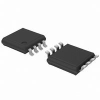
74HC2G66DP,125 NXP Semiconductors, 74HC2G66DP,125 Datasheet - Page 5

74HC2G66DP,125
Manufacturer Part Number
74HC2G66DP,125
Description
IC SWITCH DUAL SPST 8TSSOP
Manufacturer
NXP Semiconductors
Series
74HCr
Type
Analog Switchr
Datasheet
1.74HC2G66DP125.pdf
(23 pages)
Specifications of 74HC2G66DP,125
Package / Case
8-TSSOP
Function
Switch
Circuit
2 x SPST - NO
On-state Resistance
21 Ohm
Voltage Supply Source
Single Supply
Voltage - Supply, Single/dual (±)
2 V ~ 5.5 V
Current - Supply
20µA
Operating Temperature
-40°C ~ 125°C
Mounting Type
Surface Mount
Switch Configuration
SPST
On Resistance (max)
250 Ohm (Typ) @ 2 V
On Time (max)
40 ns (Typ) @ 2 V
Off Time (max)
21 ns (Typ) @ 2 V
Supply Voltage (max)
10 V
Supply Voltage (min)
2 V
Maximum Power Dissipation
300 mW
Maximum Operating Temperature
+ 125 C
Mounting Style
SMD/SMT
Minimum Operating Temperature
- 40 C
Package
8TSSOP
Maximum On Resistance
142@4.5V Ohm
Maximum Propagation Delay Bus To Bus
6.5(Typ)@2V|2(Typ)@4.5V|1.5(Typ)@6V|1.2(Typ)@9V ns
Maximum Low Level Output Current
20 mA
Maximum Turn-off Time
21(Typ)@2V ns
Maximum Turn-on Time
40(Typ)@2V ns
Switch Architecture
SPST
Power Supply Type
Single
Lead Free Status / RoHS Status
Lead free / RoHS Compliant
Lead Free Status / RoHS Status
Lead free / RoHS Compliant, Lead free / RoHS Compliant
Other names
74HC2G66DP-G
74HC2G66DP-G
935272945125
74HC2G66DP-G
935272945125
NXP Semiconductors
9. Recommended operating conditions
Table 6.
Voltages are referenced to GND (ground = 0 V).
[1]
10. Static characteristics
Table 7.
Voltages are referenced to GND (ground = 0 V).
74HC_HCT2G66
Product data sheet
Symbol Parameter
V
V
V
V
T
Δt/ΔV
Symbol Parameter
74HC2G66
V
V
I
I
I
I
I
S(OFF)
S(ON)
CC
amb
CC
I
O
SW
IH
IL
To avoid drawing V
exceed 0.4 V. If the switch current flows into pin nZ, no V
voltage drop across the switch, but the voltage at pins nY and nZ may not exceed V
HIGH-level
input voltage
LOW-level
input voltage
input leakage current
OFF-state
leakage current
ON-state
leakage current
supply current
supply voltage
input voltage
output voltage
switch voltage
ambient temperature
input transition rise
and fall rate
Recommended operating conditions
Static characteristics
CC
current out of pin nZ, when switch current flows in pin nY, the voltage drop across the bidirectional switch must not
Conditions
V
V
V
V
nE; V
Conditions
V
V
V
V
V
V
V
V
nY or nZ; V
nY or nZ; V
nE, nY and nZ = V
CC
CC
CC
CC
CC
CC
CC
CC
CC
CC
CC
CC
V
V
V
V
CC
CC
CC
CC
= 2.0 V
= 4.5 V
= 6.0 V
= 10.0 V
= 2.0 V
= 2.0 V
= 4.5 V
= 6.0 V
= 9.0 V
= 4.5 V
= 6.0 V
= 9.0 V
I
= V
All information provided in this document is subject to legal disclaimers.
= 6.0 V
= 9.0 V
= 6.0 V
= 9.0 V
CC
CC
CC
[1]
Rev. 8 — 23 September 2010
or GND
= 9.0 V; see
= 9.0 V; see
CC
CC
or GND
current will flow out of terminal nY. In this case there is no limit for the
Figure 6
Figure 7
Min
−40
2.0
0
0
0
-
-
-
-
74HC2G66; 74HCT2G66
74HC2G66
Dual single-pole single-throw analog switch
1.67
Typ
+25
5.0
-
-
-
-
-
-
3.15
Min
1.5
4.2
6.3
−40 °C to +85 °C
-
-
-
-
-
-
-
-
-
-
CC
+125
Max
10.0
V
V
V
625
139
or GND.
83
35
Typ
CC
CC
CC
1.2
2.4
3.2
4.7
0.8
2.1
2.8
4.3
0.1
0.1
-
-
-
-
[1]
Min
−40
4.5
Max
1.35
±0.1
±0.2
0
0
0
0.5
1.8
2.7
1.0
1.0
-
-
-
-
10
20
-
-
-
-
74HCT2G66
−40 °C to +125 °C Unit
1.67
Typ
+25
5.0
3.15
Min
-
-
-
-
-
-
1.5
4.2
6.3
-
-
-
-
-
-
-
-
-
-
© NXP B.V. 2010. All rights reserved.
+125
Max
V
V
V
139
5.5
CC
CC
CC
-
-
-
Max
1.35
±0.1
±0.2
0.5
1.8
2.7
1.0
1.0
20
40
-
-
-
-
Unit
V
V
V
V
°C
ns/V
ns/V
ns/V
ns/V
5 of 23
V
V
V
V
V
V
V
V
μA
μA
μA
μA
μA
μA


