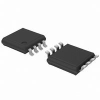
74HC2G66DP,125 NXP Semiconductors, 74HC2G66DP,125 Datasheet - Page 11

74HC2G66DP,125
Manufacturer Part Number
74HC2G66DP,125
Description
IC SWITCH DUAL SPST 8TSSOP
Manufacturer
NXP Semiconductors
Series
74HCr
Type
Analog Switchr
Datasheet
1.74HC2G66DP125.pdf
(23 pages)
Specifications of 74HC2G66DP,125
Package / Case
8-TSSOP
Function
Switch
Circuit
2 x SPST - NO
On-state Resistance
21 Ohm
Voltage Supply Source
Single Supply
Voltage - Supply, Single/dual (±)
2 V ~ 5.5 V
Current - Supply
20µA
Operating Temperature
-40°C ~ 125°C
Mounting Type
Surface Mount
Switch Configuration
SPST
On Resistance (max)
250 Ohm (Typ) @ 2 V
On Time (max)
40 ns (Typ) @ 2 V
Off Time (max)
21 ns (Typ) @ 2 V
Supply Voltage (max)
10 V
Supply Voltage (min)
2 V
Maximum Power Dissipation
300 mW
Maximum Operating Temperature
+ 125 C
Mounting Style
SMD/SMT
Minimum Operating Temperature
- 40 C
Package
8TSSOP
Maximum On Resistance
142@4.5V Ohm
Maximum Propagation Delay Bus To Bus
6.5(Typ)@2V|2(Typ)@4.5V|1.5(Typ)@6V|1.2(Typ)@9V ns
Maximum Low Level Output Current
20 mA
Maximum Turn-off Time
21(Typ)@2V ns
Maximum Turn-on Time
40(Typ)@2V ns
Switch Architecture
SPST
Power Supply Type
Single
Lead Free Status / RoHS Status
Lead free / RoHS Compliant
Lead Free Status / RoHS Status
Lead free / RoHS Compliant, Lead free / RoHS Compliant
Other names
74HC2G66DP-G
74HC2G66DP-G
935272945125
74HC2G66DP-G
935272945125
NXP Semiconductors
Table 11.
[1]
Table 12.
GND = 0 V; t
74HC_HCT2G66
Product data sheet
Type
74HC2G66
74HCT2G66
Symbol
THD
Fig 12. Test circuit for measuring switching times
There is no constraint on t
Test data is given in
Definitions for test circuit:
R
C
R
S1 = Test selection switch.
Parameter
total harmonic
distortion
T
L
L
Test data
Additional dynamic characteristics for 74HC2G66 and 74HCT2G66
r
= Load capacitance including jig and probe capacitance.
= Load resistance.
= Termination resistance should be equal to output impedance Z
= t
f
11.2 Additional dynamic characteristics
Input
V
GND to V
GND to 3 V
= 6.0 ns; C
I
CC
r
, t
Table
L
f
= 50 pF; unless otherwise specified. All typical values are measured at T
with a 50 % duty factor when measuring f
t
6 ns
6 ns
negative
positive
r
, t
11.
pulse
pulse
Conditions
f
f
i
i
f
[1]
0 V
0 V
= 1 kHz; R
= 10 kHz; R
V
V
V
V
V
V
G
I
I
CC
CC
CC
CC
90 %
10 %
= 4.5 V; V
= 9.0 V; V
= 4.5 V; V
= 9.0 V; V
All information provided in this document is subject to legal disclaimers.
V I
L
Load
C
50 pF
50 pF
L
Rev. 8 — 23 September 2010
t
t
= 10 kΩ; see
f
r
L
= 10 kΩ; see
V
V
M
M
I
I
I
I
R T
10 %
90 %
= 4.0 V (p-p)
= 8.0 V (p-p)
= 4.0 V (p-p)
= 8.0 V (p-p)
DUT
V
CC
t
t
Figure 13
W
W
R
1 kΩ
1 kΩ
Figure 13
L
V O
max
74HC2G66; 74HCT2G66
o
.
of the pulse generator.
Dual single-pole single-throw analog switch
V
V
M
M
C L
t
t
r
f
R L
S1 position
t
open
open
PHL
Min
-
-
-
-
S1
, t
001aad983
PLH
V
CC
open
t
GND
GND
Typ
0.04
0.02
0.12
0.06
PZH
, t
PHZ
amb
© NXP B.V. 2010. All rights reserved.
= 25
Max
-
-
-
-
t
V
V
PZL
CC
CC
°
C.
, t
PLZ
Unit
%
%
%
%
%
11 of 23


