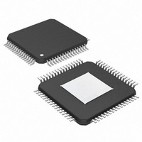
MAX3880ECB+D Maxim Integrated Products, MAX3880ECB+D Datasheet - Page 8

MAX3880ECB+D
Manufacturer Part Number
MAX3880ECB+D
Description
IC 1:16 DESERIALIZER 64-TQFP
Manufacturer
Maxim Integrated Products
Datasheet
1.MAX3880ECBD.pdf
(12 pages)
Specifications of MAX3880ECB+D
Function
Deserializer
Data Rate
2.5Gbps
Input Type
Serial
Output Type
LVDS
Number Of Inputs
1
Number Of Outputs
16
Voltage - Supply
3 V ~ 3.6 V
Operating Temperature
-40°C ~ 85°C
Mounting Type
Surface Mount
Package / Case
64-TQFP Exposed Pad, 64-eTQFP, 64-HTQFP, 64-VQFP
Lead Free Status / RoHS Status
Lead free / RoHS Compliant
+3.3V, 2.488Gbps, SDH/SONET
1:16 Deserializer with Clock Recovery
Figure 5. Timing Parameters
The MAX3880 features LVDS inputs and outputs for
interfacing with high-speed digital circuitry. The LVDS
standard is based on the IEEE 1596.3 LVDS specifica-
tion. This technology uses 500mVp-p to 800mVp-p dif-
ferential low-voltage swings to achieve fast transition
times, minimize power dissipation, and improve noise
immunity. For proper operation, the parallel clock and
data LVDS outputs (PCLK+, PCLK-, PD_+, PD_-)
require 100Ω differential DC termination between the
positive and negative outputs. Do not terminate these
outputs to ground. The synchronization LVDS inputs
(SYNC+, SYNC-) are internally terminated with 100Ω
differential input resistance and therefore do not require
external termination.
When the received data amplitude is higher than
50mVp-p, the MAX3880 provides a typical jitter toler-
ance of 0.46 UI at jitter frequencies greater than
10MHz. The SDH/SONET jitter tolerance specification is
0.15UI, leaving a jitter allowance of 0.31UI for receiver
preamplifier and postamplifier design.
The BER is better than 1 x 10
greater than 9.5mVp-p. At 25mVp-p, jitter tolerance will
be degraded, but will still be above the SDH/SONET
requirement. Trade-offs can be made between jitter tol-
erance and input sensitivity according to the specific
application. See the Typical Operating Characteristics
for Jitter Tolerance and BER vs. Input Voltage graphs.
8
PD0–PD15
NOTE: SIGNALS SHOWN ARE DIFFERENTIAL. FOR EXAMPLE, PCLK = (PCLK+) - (PCLK-).
_______________________________________________________________________________________
PCLK
Low-Voltage Differential-Signal (LVDS)
t
Jitter Tolerance and Input
CLK-Q
Design Procedure
Sensitivity Trade-Offs
Inputs and Outputs
-10
for input signals
The MAX3880 has a low phase and frequency drift in
the absence of data transitions. As a result, long runs of
consecutive zeros and ones can be tolerated while
maintaining a BER of 1 x 10
tested using a 2
(PRBS), substituting a long run of zeros to simulate the
worst case. A CID tolerance of greater than 2,000 bits
is typical.
The internal clock is aligned to the center of the data
eye. For specific applications, this sampling position
can be shifted using the PHADJ inputs to optimize BER
performance. The PHADJ inputs operate with differen-
tial input voltages up to ±1.5V. A simple resistor-divider
with a bypass capacitor is sufficient to set these levels
(Figure 6). When the PHADJ inputs are not used, they
should be tied directly to V
The MAX3880 is designed to allow system loopback
testing. The user can connect a serializer output
(MAX3890) in a transceiver directly to the SLBI+ and
SLBI- inputs of the MAX3880 for system diagnostics. To
select the SLBI± inputs, apply a TTL logic high to the
SIS pin.
Figure 6. Phase-Adjust Resistor-Divider
Consecutive Identical Digits (CIDs)
3.3V
Applications Information
13
- 1 pseudorandom bit stream
PHADJ+ (PIN 5)
PHADJ- (PIN 6)
CC
MAX3880
.
-10
. The CID tolerance is
System Loopback
Phase Adjust


