MAX3880ECB+D Maxim Integrated Products, MAX3880ECB+D Datasheet - Page 5
MAX3880ECB+D
Manufacturer Part Number
MAX3880ECB+D
Description
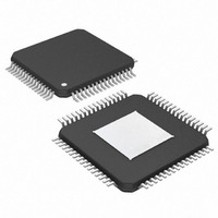
IC 1:16 DESERIALIZER 64-TQFP
Manufacturer
Maxim Integrated Products
Datasheet
1.MAX3880ECBD.pdf
(12 pages)
Specifications of MAX3880ECB+D
Function
Deserializer
Data Rate
2.5Gbps
Input Type
Serial
Output Type
LVDS
Number Of Inputs
1
Number Of Outputs
16
Voltage - Supply
3 V ~ 3.6 V
Operating Temperature
-40°C ~ 85°C
Mounting Type
Surface Mount
Package / Case
64-TQFP Exposed Pad, 64-eTQFP, 64-HTQFP, 64-VQFP
Lead Free Status / RoHS Status
Lead free / RoHS Compliant


1, 17, 25, 33,
52, 54, 58, 60
53, 55, 59, 61
4, 7, 10, 13,
41, 49, 56,
24, 32, 40,
20, 22, 26,
28, 30, 34,
36, 38, 42,
44, 46, 50,
21, 23, 27,
29, 31, 35,
37, 39, 43,
45, 47, 51,
62, 64
48, 57
PIN
EP
11
12
14
15
16
18
19
63
2
3
5
6
8
9
Exposed Pad
PHADJ+
PD0+ to
PHADJ-
SYNC+
PD0- to
PCLK+
PD15+
NAME
SYNC-
PCLK-
SLBI+
PD15-
_______________________________________________________________________________________
SLBI-
GND
SDI+
FIL+
SDI-
V
LOL
FIL-
SIS
CC
1:16 Deserializer with Clock Recovery
Ground
Positive Filter Input. PLL loop filter connection. Connect a 1.0µF capacitor between FIL+ and FIL-.
Negative Filter Input. PLL loop filter connection. Connect a 1.0µF capacitor between FIL+ and FIL-.
+3.3V Supply Voltage
Positive Phase-Adjust Input. Used to optimally align internal PLL phase. Connect to V
used.
Negative Phase-Adjust Input. Used to optimally align internal PLL phase. Connect to V
used.
Positive Serial Data Input. 2.488Gbps data stream.
Negative Serial Data Input. 2.488Gbps data stream.
Positive System Loopback Input. 2.488Gbps data stream.
Negative System Loopback Input. 2.488Gbps data stream.
Signal Input Selection. TTL low for normal data input (SDI). TTL high for system loopback input
(SLBI).
Negative Synchronizing Pulse LVDS Input. Pulse the SYNC signal high for at least four serial-data
bit periods (1.6ns) to shift the data alignment by dropping 1 bit.
Positive Synchronizing Pulse LVDS Input. Pulse the SYNC signal high for at least four serial-data
bit periods (1.6ns) to shift the data alignment by dropping 1 bit.
Negative Parallel Clock LVDS Output
Positive Parallel Clock LVDS Output
Negative Parallel Data LVDS Outputs. Data is updated on the negative transition of the PCLK
signal (Figure 5).
Positive Parallel Data LVDS Outputs. Data is updated on the negative transition of the PCLK
signal (Figure 5).
Loss-of-Lock Output. PLL loss-of-lock monitor, TTL active low (internal 10kΩ pull-up resistor). The
LOL monitor is valid only when a data stream is present on the inputs to the MAX3880.
Ground. This must be soldered to a circuit board for proper thermal performance (see Package
Information).
+3.3V, 2.488Gbps, SDH/SONET
FUNCTION
Pin Description
CC
CC
if not
if not
5
Related parts for MAX3880ECB+D
Image
Part Number
Description
Manufacturer
Datasheet
Request
R

Part Number:
Description:
MAX7528KCWPMaxim Integrated Products [CMOS Dual 8-Bit Buffered Multiplying DACs]
Manufacturer:
Maxim Integrated Products
Datasheet:
Part Number:
Description:
Single +5V, fully integrated, 1.25Gbps laser diode driver.
Manufacturer:
Maxim Integrated Products
Datasheet:
Part Number:
Description:
Single +5V, fully integrated, 155Mbps laser diode driver.
Manufacturer:
Maxim Integrated Products
Datasheet:
Part Number:
Description:
VRD11/VRD10, K8 Rev F 2/3/4-Phase PWM Controllers with Integrated Dual MOSFET Drivers
Manufacturer:
Maxim Integrated Products
Datasheet:
Part Number:
Description:
Highly Integrated Level 2 SMBus Battery Chargers
Manufacturer:
Maxim Integrated Products
Datasheet:
Part Number:
Description:
Current Monitor and Accumulator with Integrated Sense Resistor; ; Temperature Range: -40°C to +85°C
Manufacturer:
Maxim Integrated Products
Part Number:
Description:
TSSOP 14/A�/RS-485 Transceivers with Integrated 100O/120O Termination Resis
Manufacturer:
Maxim Integrated Products
Part Number:
Description:
TSSOP 14/A�/RS-485 Transceivers with Integrated 100O/120O Termination Resis
Manufacturer:
Maxim Integrated Products
Part Number:
Description:
QFN 16/A�/AC-DC and DC-DC Peak-Current-Mode Converters with Integrated Step
Manufacturer:
Maxim Integrated Products
Part Number:
Description:
TDFN/A/65V, 1A, 600KHZ, SYNCHRONOUS STEP-DOWN REGULATOR WITH INTEGRATED SWI
Manufacturer:
Maxim Integrated Products
Part Number:
Description:
Integrated Temperature Controller f
Manufacturer:
Maxim Integrated Products
Part Number:
Description:
SOT23-6/I�/45MHz to 650MHz, Integrated IF VCOs with Differential Output
Manufacturer:
Maxim Integrated Products
Part Number:
Description:
SOT23-6/I�/45MHz to 650MHz, Integrated IF VCOs with Differential Output
Manufacturer:
Maxim Integrated Products
Part Number:
Description:
EVALUATION KIT/2.4GHZ TO 2.5GHZ 802.11G/B RF TRANSCEIVER WITH INTEGRATED PA
Manufacturer:
Maxim Integrated Products
Part Number:
Description:
QFN/E/DUAL PCIE/SATA HIGH SPEED SWITCH WITH INTEGRATED BIAS RESISTOR
Manufacturer:
Maxim Integrated Products
Datasheet: